ATmega48/88/168
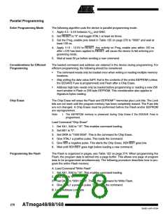
1. Set XA1, XA0 to “00”. This enables address loading.
2. Set BS1 to “0”. This selects low address.
3. Set DATA = Address low byte (0x00 - 0xFF).
4. Give XTAL1 a positive pulse. This loads the address low byte.
C. Load Data Low Byte
1. Set XA1, XA0 to “01”. This enables data loading.
2. Set DATA = Data low byte (0x00 - 0xFF).
3. Give XTAL1 a positive pulse. This loads the data byte.
D. Load Data High Byte
1. Set BS1 to “1”. This selects high data byte.
2. Set XA1, XA0 to “01”. This enables data loading.
3. Set DATA = Data high byte (0x00 - 0xFF).
4. Give XTAL1 a positive pulse. This loads the data byte.
E. Latch Data
1. Set BS1 to “1”. This selects high data byte.
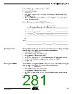
2. Give PAGEL a positive pulse. This latches the data bytes. (See Figure 121 for
signal waveforms)
F. Repeat B through E until the entire buffer is filled or until all data within the page is
loaded.
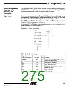
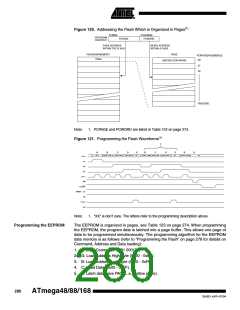
While the lower bits in the address are mapped to words within the page, the higher bits
address the pages within the FLASH. This is illustrated in Figure 120 on page 280. Note
that if less than eight bits are required to address words in the page (pagesize < 256),
the most significant bit(s) in the address low byte are used to address the page when
performing a Page Write.
G. Load Address High byte
1. Set XA1, XA0 to “00”. This enables address loading.
2. Set BS1 to “1”. This selects high address.
3. Set DATA = Address high byte (0x00 - 0xFF).
4. Give XTAL1 a positive pulse. This loads the address high byte.
H. Program Page
1. Give WR a negative pulse. This starts programming of the entire page of data.
RDY/BSY goes low.
2. Wait until RDY/BSY goes high (See Figure 121 for signal waveforms).
I. Repeat B through H until the entire Flash is programmed or until all data has been
programmed.
J. End Page Programming
1. 1. Set XA1, XA0 to “10”. This enables command loading.
2. Set DATA to “0000 0000”. This is the command for No Operation.
3. Give XTAL1 a positive pulse. This loads the command, and the internal write sig-
nals are reset.
279
2545D–AVR–07/04

 ATMEL [ ATMEL ]