Table 124. Pin Name Mapping (Continued)
Signal Name in
Programming Mode
Pin Name
I/O Function
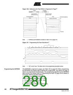
Program memory and EEPROM Data
Page Load
PAGEL
PD7
I
I
Byte Select 2 (“0” selects Low byte, “1”
selects 2’nd High byte)
BS2
PC2
Bi-directional Data bus (Output when OE is
low)
DATA
{PC[1:0]: PB[5:0]} I/O
Table 125. Pin Values Used to Enter Programming Mode
Pin
PAGEL
XA1
Symbol
Value
Prog_enable[3]
Prog_enable[2]
Prog_enable[1]
Prog_enable[0]
0
0
0
0
XA0
BS1
Table 126. XA1 and XA0 Coding
XA1
XA0
Action when XTAL1 is Pulsed
0
0
Load Flash or EEPROM Address (High or low address byte
determined by BS1).
0
1
1
1
0
1
Load Data (High or Low data byte for Flash determined by BS1).
Load Command
No Action, Idle
Table 127. Command Byte Bit Coding
Command Byte
1000 0000
0100 0000
0010 0000
0001 0000
0001 0001
0000 1000
0000 0100
0000 0010
0000 0011
Command Executed
Chip Erase
Write Fuse bits
Write Lock bits
Write Flash
Write EEPROM
Read Signature Bytes and Calibration byte
Read Fuse and Lock bits
Read Flash
Read EEPROM
276
ATmega48/88/168
2545D–AVR–07/04

 ATMEL [ ATMEL ]