ATmega48/88/168
•
•
Capacitors connected to the RESET pin must be disconnected when using
debugWire.
All external reset sources must be disconnected.
Software Break Points
debugWIRE supports Program memory Break Points by the AVR Break instruction. Set-
ting a Break Point in AVR Studio® will insert a BREAK instruction in the Program
memory. The instruction replaced by the BREAK instruction will be stored. When pro-
gram execution is continued, the stored instruction will be executed before continuing
from the Program memory. A break can be inserted manually by putting the BREAK
instruction in the program.
The Flash must be re-programmed each time a Break Point is changed. This is auto-
matically handled by AVR Studio through the debugWIRE interface. The use of Break
Points will therefore reduce the Flash Data retention. Devices used for debugging pur-
poses should not be shipped to end customers.
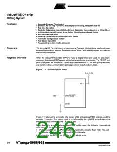
Limitations of
debugWIRE
The debugWIRE communication pin (dW) is physically located on the same pin as
External Reset (RESET). An External Reset source is therefore not supported when the
debugWIRE is enabled.
The debugWIRE system accurately emulates all I/O functions when running at full
speed, i.e., when the program in the CPU is running. When the CPU is stopped, care
must be taken while accessing some of the I/O Registers via the debugger (AVR
Studio).
A programmed DWEN Fuse enables some parts of the clock system to be running in all
sleep modes. This will increase the power consumption while in sleep. Thus, the DWEN
Fuse should be disabled when debugWire is not used.
debugWIRE Related
The following section describes the registers used with the debugWire.
Register in I/O Memory
debugWire Data Register –
DWDR
Bit
7
6
5
4
3
2
1
0
DWDR[7:0]
DWDR
Read/Write
Initial Value
R/W
0
R/W
0
R/W
0
R/W
0
R/W
0
R/W
0
R/W
0
R/W
0
The DWDR Register provides a communication channel from the running program in
the MCU to the debugger. This register is only accessible by the debugWIRE and can
therefore not be used as a general purpose register in the normal operations.
247
2545D–AVR–07/04

 ATMEL [ ATMEL ]