debugWIRE On-chip
Debug System
Features
• Complete Program Flow Control
• Emulates All On-chip Functions, Both Digital and Analog, except RESET Pin
• Real-time Operation
• Symbolic Debugging Support (Both at C and Assembler Source Level, or for Other HLLs)
• Unlimited Number of Program Break Points (Using Software Break Points)
• Non-intrusive Operation
• Electrical Characteristics Identical to Real Device
• Automatic Configuration System
• High-Speed Operation
• Programming of Non-volatile Memories
Overview
The debugWIRE On-chip debug system uses a One-wire, bi-directional interface to con-
trol the program flow, execute AVR instructions in the CPU and to program the different
non-volatile memories.
Physical Interface
When the debugWIRE Enable (DWEN) Fuse is programmed and Lock bits are unpro-
grammed, the debugWIRE system within the target device is activated. The RESET port
pin is configured as a wire-AND (open-drain) bi-directional I/O pin with pull-up enabled
and becomes the communication gateway between target and emulator.
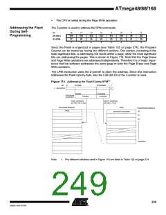
Figure 114. The debugWIRE Setup
1.8 - 5.5V
VCC
dW
dW(RESET)
GND
Figure 114 shows the schematic of a target MCU, with debugWIRE enabled, and the
emulator connector. The system clock is not affected by debugWIRE and will always be
the clock source selected by the CKSEL Fuses.
When designing a system where debugWIRE will be used, the following observations
must be made for correct operation:
•
Pull-up resistors on the dW/(RESET) line must not be smaller than 10kΩ. The pull-
up resistor is not required for debugWIRE functionality.
•
Connecting the RESET pin directly to VCC will not work.
246
ATmega48/88/168
2545D–AVR–07/04

 ATMEL [ ATMEL ]