mode the ADC will perform successive conversions independently of whether the ADC
Interrupt Flag, ADIF is cleared or not.
If Auto Triggering is enabled, single conversions can be started by writing ADSC in
ADCSRA to one. ADSC can also be used to determine if a conversion is in progress.
The ADSC bit will be read as one during a conversion, independently of how the conver-
sion was started.
Prescaling and
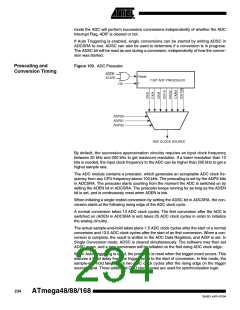
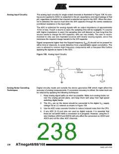
Figure 103. ADC Prescaler
Conversion Timing
ADEN
START
Reset
7-BIT ADC PRESCALER
CK
ADPS0
ADPS1
ADPS2
ADC CLOCK SOURCE
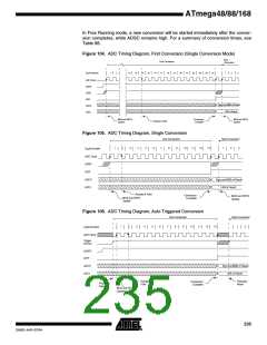
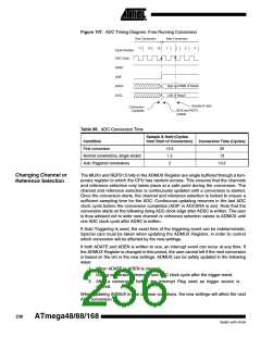
By default, the successive approximation circuitry requires an input clock frequency
between 50 kHz and 200 kHz to get maximum resolution. If a lower resolution than 10
bits is needed, the input clock frequency to the ADC can be higher than 200 kHz to get a
higher sample rate.
The ADC module contains a prescaler, which generates an acceptable ADC clock fre-
quency from any CPU frequency above 100 kHz. The prescaling is set by the ADPS bits
in ADCSRA. The prescaler starts counting from the moment the ADC is switched on by
setting the ADEN bit in ADCSRA. The prescaler keeps running for as long as the ADEN
bit is set, and is continuously reset when ADEN is low.
When initiating a single ended conversion by setting the ADSC bit in ADCSRA, the con-
version starts at the following rising edge of the ADC clock cycle.
A normal conversion takes 13 ADC clock cycles. The first conversion after the ADC is
switched on (ADEN in ADCSRA is set) takes 25 ADC clock cycles in order to initialize
the analog circuitry.
The actual sample-and-hold takes place 1.5 ADC clock cycles after the start of a normal
conversion and 13.5 ADC clock cycles after the start of an first conversion. When a con-
version is complete, the result is written to the ADC Data Registers, and ADIF is set. In
Single Conversion mode, ADSC is cleared simultaneously. The software may then set
ADSC again, and a new conversion will be initiated on the first rising ADC clock edge.
When Auto Triggering is used, the prescaler is reset when the trigger event occurs. This
assures a fixed delay from the trigger event to the start of conversion. In this mode, the
sample-and-hold takes place two ADC clock cycles after the rising edge on the trigger
source signal. Three additional CPU clock cycles are used for synchronization logic.
234
ATmega48/88/168
2545D–AVR–07/04

 ATMEL [ ATMEL ]