The IEEE std. 1149.1 also specifies an optional TAP signal; TRST – Test ReSeT –
which is not provided.
When the JTAGEN Fuse is unprogrammed, these four TAP pins are normal port pins,
and the TAP controller is in reset. When programmed, the input TAP signals are inter-
nally pulled high and the JTAG is enabled for Boundary-scan and programming. The
device is shipped with this fuse programmed.
For the On-chip Debug system, in addition to the JTAG interface pins, the RESET pin is
monitored by the debugger to be able to detect external reset sources. The debugger
can also pull the RESET pin low to reset the whole system, assuming only open collec-
tors on the reset line are used in the application.
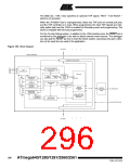
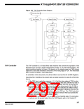
Figure 129. Block Diagram
I/O PORT 0
DEVICE BOUNDARY
BOUNDARY SCAN CHAIN
TDI
JTAG PROGRAMMING
INTERFACE
TDO
TCK
TMS
TAP
CONTROLLER
AVR CPU
INTERNAL
FLASH
MEMORY
Address
Data
SCAN
CHAIN
PC
Instruction
INSTRUCTION
REGISTER
ID
REGISTER
BREAKPOINT
UNIT
M
U
X
FLOW CONTROL
UNIT
BYPASS
REGISTER
DIGITAL
PERIPHERAL
UNITS
ANALOG
PERIPHERIAL
UNITS
Analog inputs
BREAKPOINT
SCAN CHAIN
JTAG / AVR CORE
COMMUNICATION
INTERFACE
ADDRESS
DECODER
OCD STATUS
AND CONTROL
Control & Clock lines
I/O PORT n
296
ATmega640/1280/1281/2560/2561
2549A–AVR–03/05

 ATMEL [ ATMEL ]