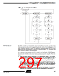
state. The Exit-IR, Pause-IR, and Exit2-IR states are only used for navigating the
state machine.
•
•
At the TMS input, apply the sequence 1, 0, 0 at the rising edges of TCK to enter the
Shift Data Register – Shift-DR state. While in this state, upload the selected Data
Register (selected by the present JTAG instruction in the JTAG Instruction Register)
from the TDI input at the rising edge of TCK. In order to remain in the Shift-DR state,
the TMS input must be held low during input of all bits except the MSB. The MSB of
the data is shifted in when this state is left by setting TMS high. While the Data
Register is shifted in from the TDI pin, the parallel inputs to the Data Register
captured in the Capture-DR state is shifted out on the TDO pin.
Apply the TMS sequence 1, 1, 0 to re-enter the Run-Test/Idle state. If the selected
Data Register has a latched parallel-output, the latching takes place in the Update-
DR state. The Exit-DR, Pause-DR, and Exit2-DR states are only used for navigating
the state machine.
As shown in the state diagram, the Run-Test/Idle state need not be entered between
selecting JTAG instruction and using Data Registers, and some JTAG instructions may
select certain functions to be performed in the Run-Test/Idle, making it unsuitable as an
Idle state.
Note:
Independent of the initial state of the TAP Controller, the Test-Logic-Reset state can
always be entered by holding TMS high for five TCK clock periods.
For detailed information on the JTAG specification, refer to the literature listed in “Bibli-
ography” on page 300.
Using the Boundary-
scan Chain
A complete description of the Boundary-scan capabilities are given in the section “IEEE
1149.1 (JTAG) Boundary-scan” on page 301.
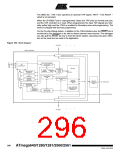
Using the On-chip Debug As shown in Figure 129, the hardware support for On-chip Debugging consists mainly of
System
•
A scan chain on the interface between the internal AVR CPU and the internal
peripheral units.
•
•
Break Point unit.
Communication interface between the CPU and JTAG system.
All read or modify/write operations needed for implementing the Debugger are done by
applying AVR instructions via the internal AVR CPU Scan Chain. The CPU sends the
result to an I/O memory mapped location which is part of the communication interface
between the CPU and the JTAG system.
The Break Point Unit implements Break on Change of Program Flow, Single Step
Break, two Program Memory Break Points, and two combined Break Points. Together,
the four Break Points can be configured as either:
•
•
•
•
4 single Program Memory Break Points.
3 Single Program Memory Break Point + 1 single Data Memory Break Point.
2 single Program Memory Break Points + 2 single Data Memory Break Points.
2 single Program Memory Break Points + 1 Program Memory Break Point with mask
(“range Break Point”).
•
2 single Program Memory Break Points + 1 Data Memory Break Point with mask
(“range Break Point”).
A debugger, like the AVR Studio, may however use one or more of these resources for
its internal purpose, leaving less flexibility to the end-user.
298
ATmega640/1280/1281/2560/2561
2549A–AVR–03/05

 ATMEL [ ATMEL ]