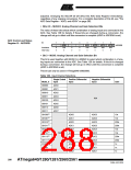
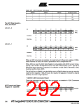
Table 127. ADC Prescaler Selections
ADPS2
ADPS1
ADPS0
Division Factor
1
1
1
0
1
1
1
0
1
32
64
128
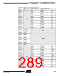
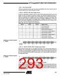
The ADC Data Register –
ADCL and ADCH
ADLAR = 0
Bit
15
14
13
12
11
10
9
8
–
–
–
–
–
–
ADC9
ADC8
ADCH
ADCL
ADC7
ADC6
ADC5
ADC4
ADC3
ADC2
ADC1
ADC0
7
R
R
0
6
R
R
0
5
R
R
0
4
R
R
0
3
R
R
0
2
R
R
0
1
R
R
0
0
R
R
0
Read/Write
Initial Value
0
0
0
0
0
0
0
0
ADLAR = 1
Bit
15
14
13
12
11
10
9
8
ADC9
ADC8
ADC7
ADC6
ADC5
ADC4
ADC3
ADC2
ADCH
ADCL
ADC1
ADC0
–
5
–
4
–
3
–
2
–
1
–
0
7
R
R
0
6
R
R
0
Read/Write
Initial Value
R
R
0
R
R
0
R
R
0
R
R
0
R
R
0
R
R
0
0
0
0
0
0
0
0
0
When an ADC conversion is complete, the result is found in these two registers. If differ-
ential channels are used, the result is presented in two’s complement form.
When ADCL is read, the ADC Data Register is not updated until ADCH is read. Conse-
quently, if the result is left adjusted and no more than 8-bit precision (7 bit + sign bit for
differential input channels) is required, it is sufficient to read ADCH. Otherwise, ADCL
must be read first, then ADCH.
The ADLAR bit in ADMUX, and the MUXn bits in ADMUX affect the way the result is
read from the registers. If ADLAR is set, the result is left adjusted. If ADLAR is cleared
(default), the result is right adjusted.
• ADC9:0: ADC Conversion Result
These bits represent the result from the conversion, as detailed in “ADC Conversion
Result” on page 286.
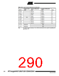
ADC Control and Status
Register B – ADCSRB
Bit
7
–
6
ACME
R/W
0
5
–
4
–
3
MUX5
R/W
0
2
ADTS2
R/W
0
1
ADTS1
R/W
0
0
ADTS0
R/W
0
ADCSRB
Read/Write
Initial Value
R
0
R
0
R
0
292
ATmega640/1280/1281/2560/2561
2549A–AVR–03/05

 ATMEL [ ATMEL ]