ATmega640/1280/1281/2560/2561
• Bit 7 – Res: Reserved Bit
This bit is reserved for future use. To ensure compatibility with future devices, this bit
must be written to zero when ADCSRB is written.
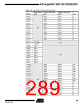
• Bit 2:0 – ADTS2:0: ADC Auto Trigger Source
If ADATE in ADCSRA is written to one, the value of these bits selects which source will
trigger an ADC conversion. If ADATE is cleared, the ADTS2:0 settings will have no
effect. A conversion will be triggered by the rising edge of the selected Interrupt Flag.
Note that switching from a trigger source that is cleared to a trigger source that is set,
will generate a positive edge on the trigger signal. If ADEN in ADCSRA is set, this will
start a conversion. Switching to Free Running mode (ADTS[2:0]=0) will not cause a trig-
ger event, even if the ADC Interrupt Flag is set.
Table 128. ADC Auto Trigger Source Selections
ADTS2
ADTS1
ADTS0
Trigger Source
0
0
0
0
1
1
1
1
0
0
1
1
0
0
1
1
0
1
0
1
0
1
0
1
Free Running mode
Analog Comparator
External Interrupt Request 0
Timer/Counter0 Compare Match A
Timer/Counter0 Overflow
Timer/Counter1 Compare Match B
Timer/Counter1 Overflow
Timer/Counter1 Capture Event
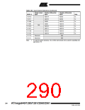
Digital Input Disable Register
0 – DIDR0
Bit
7
ADC7D
R/W
0
6
ADC6D
R/W
0
5
ADC5D
R/W
0
4
ADC4D
R/W
0
3
ADC3D
R/W
0
2
ADC2D
R/W
0
1
ADC1D
R/W
0
0
ADC0D
R/W
0
DIDR0
Read/Write
Initial Value
• Bit 7..0 – ADC7D..ADC0D: ADC7..0 Digital Input Disable
When this bit is written logic one, the digital input buffer on the corresponding ADC pin is
disabled. The corresponding PIN Register bit will always read as zero when this bit is
set. When an analog signal is applied to the ADC7..0 pin and the digital input from this
pin is not needed, this bit should be written logic one to reduce power consumption in
the digital input buffer.
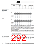
Digital Input Disable Register
2 – DIDR2
Bit
7
ADC15D
R/W
6
ADC14D
R/W
5
ADC13D
R/W
4
ADC12D
R/W
3
ADC11D
R/W
2
ADC10D
R/W
1
ADC9D
R/W
0
0
ADC8D
R/W
0
DIDR2
Read/Write
Initial Value
0
0
0
0
0
0
• Bit 7..0 – ADC15D..ADC8D: ADC15..8 Digital Input Disable
When this bit is written logic one, the digital input buffer on the corresponding ADC pin is
disabled. The corresponding PIN Register bit will always read as zero when this bit is
set. When an analog signal is applied to the ADC15..8 pin and the digital input from this
pin is not needed, this bit should be written logic one to reduce power consumption in
the digital input buffer.
293
2549A–AVR–03/05

 ATMEL [ ATMEL ]