ATmega640/1280/1281/2560/2561
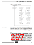
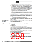
Figure 130. TAP Controller State Diagram
1
Test-Logic-Reset
0
1
1
1
0
Run-Test/Idle
Select-DR Scan
Select-IR Scan
0
0
1
1
Capture-DR
Capture-IR
0
0
Shift-IR
1
Shift-DR
0
0
1
Exit1-DR
0
1
1
Exit1-IR
0
Pause-DR
1
0
Pause-IR
1
0
0
0
Exit2-DR
1
Exit2-IR
1
Update-DR
Update-IR
1
1
0
0
TAP Controller
The TAP controller is a 16-state finite state machine that controls the operation of the
Boundary-scan circuitry, JTAG programming circuitry, or On-chip Debug system. The
state transitions depicted in Figure 130 depend on the signal present on TMS (shown
adjacent to each state transition) at the time of the rising edge at TCK. The initial state
after a Power-on Reset is Test-Logic-Reset.
As a definition in this document, the LSB is shifted in and out first for all Shift Registers.
Assuming Run-Test/Idle is the present state, a typical scenario for using the JTAG inter-
face is:
•
At the TMS input, apply the sequence 1, 1, 0, 0 at the rising edges of TCK to enter
the Shift Instruction Register – Shift-IR state. While in this state, shift the four bits of
the JTAG instructions into the JTAG Instruction Register from the TDI input at the
rising edge of TCK. The TMS input must be held low during input of the 3 LSBs in
order to remain in the Shift-IR state. The MSB of the instruction is shifted in when
this state is left by setting TMS high. While the instruction is shifted in from the TDI
pin, the captured IR-state 0x01 is shifted out on the TDO pin. The JTAG Instruction
selects a particular Data Register as path between TDI and TDO and controls the
circuitry surrounding the selected Data Register.
•
Apply the TMS sequence 1, 1, 0 to re-enter the Run-Test/Idle state. The instruction
is latched onto the parallel output from the Shift Register path in the Update-IR
297
2549A–AVR–03/05

 ATMEL [ ATMEL ]