ATmega640/1280/1281/2560/2561
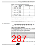
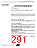
ADC Control and Status
Register A – ADCSRA
Bit
7
ADEN
R/W
0
6
ADSC
R/W
0
5
ADATE
R/W
0
4
ADIF
R/W
0
3
ADIE
R/W
0
2
ADPS2
R/W
0
1
ADPS1
R/W
0
0
ADPS0
R/W
0
ADCSRA
Read/Write
Initial Value
• Bit 7 – ADEN: ADC Enable
Writing this bit to one enables the ADC. By writing it to zero, the ADC is turned off. Turn-
ing the ADC off while a conversion is in progress, will terminate this conversion.
• Bit 6 – ADSC: ADC Start Conversion
In Single Conversion mode, write this bit to one to start each conversion. In Free Run-
ning mode, write this bit to one to start the first conversion. The first conversion after
ADSC has been written after the ADC has been enabled, or if ADSC is written at the
same time as the ADC is enabled, will take 25 ADC clock cycles instead of the normal
13. This first conversion performs initialization of the ADC.
ADSC will read as one as long as a conversion is in progress. When the conversion is
complete, it returns to zero. Writing zero to this bit has no effect.
• Bit 5 – ADATE: ADC Auto Trigger Enable
When this bit is written to one, Auto Triggering of the ADC is enabled. The ADC will start
a conversion on a positive edge of the selected trigger signal. The trigger source is
selected by setting the ADC Trigger Select bits, ADTS in ADCSRB.
• Bit 4 – ADIF: ADC Interrupt Flag
This bit is set when an ADC conversion completes and the Data Registers are updated.
The ADC Conversion Complete Interrupt is executed if the ADIE bit and the I-bit in
SREG are set. ADIF is cleared by hardware when executing the corresponding interrupt
handling vector. Alternatively, ADIF is cleared by writing a logical one to the flag.
Beware that if doing a Read-Modify-Write on ADCSRA, a pending interrupt can be dis-
abled. This also applies if the SBI and CBI instructions are used.
• Bit 3 – ADIE: ADC Interrupt Enable
When this bit is written to one and the I-bit in SREG is set, the ADC Conversion Com-
plete Interrupt is activated.
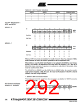
• Bits 2:0 – ADPS2:0: ADC Prescaler Select Bits
These bits determine the division factor between the XTAL frequency and the input
clock to the ADC.
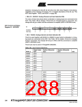
Table 127. ADC Prescaler Selections
ADPS2
ADPS1
ADPS0
Division Factor
0
0
0
0
1
0
0
1
1
0
0
1
0
1
0
2
2
4
8
16
291
2549A–AVR–03/05

 ATMEL [ ATMEL ]