adjusted. Changing the ADLAR bit will affect the ADC Data Register immediately,
regardless of any ongoing conversions. For a complete description of this bit, see “The
ADC Data Register – ADCL and ADCH” on page 292.
• Bits 4:0 – MUX4:0: Analog Channel and Gain Selection Bits
The value of these bits selects which combination of analog inputs are connected to the
ADC. See Table 126 for details. If these bits are changed during a conversion, the
change will not go in effect until this conversion is complete (ADIF in ADCSRA is set)
ADC Control and Status
Register B – ADCSRB
Bit
7
–
6
ACME
R/W
0
5
–
4
–
3
MUX5
R/W
0
2
ADTS2
R/W
0
1
ADTS1
R/W
0
0
ADTS0
R/W
0
ADCSRB
Read/Write
Initial Value
R
0
R
0
R
0
• Bit 3 – MUX5: Analog Channel and Gain Selection Bit
This bit is used together with MUX4:0 in ADMUX to select which combination in of ana-
log inputs are connected to the ADC. See Table 126 for details. If this bit is changed
during a conversion, the change will not go in effect until this conversion is complete
(ADIF in ADCSRA is set).
This bit can only be used in ATmega640/1280/2560.
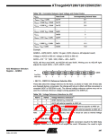
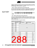
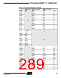
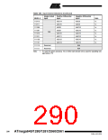
Table 126. Input Channel Selections
Single Ended
Input
Positive Differential
Input
Negative Differential
Input
MUX5..0
000000
Gain
ADC0
ADC1
ADC2
ADC3
ADC4
ADC5
ADC6
ADC7
000001
000010
000011
N/A
000100
000101
000110
000111
001000(1)
001001(1)
001010(1)
001011(1)
001100(1)
001101(1)
001110(1)
001111(1)
010000
ADC0
ADC1
ADC0
ADC1
ADC2
ADC3
ADC2
ADC3
ADC0
ADC1
ADC2
ADC0
ADC0
ADC0
ADC0
ADC2
ADC2
ADC2
ADC2
ADC1
ADC1
ADC1
10x
10x
200x
200x
10x
10x
200x
200x
1x
N/A
010001
1x
010010
1x
288
ATmega640/1280/1281/2560/2561
2549A–AVR–03/05

 ATMEL [ ATMEL ]