Offset Compensation
Schemes
The stage has a built-in offset cancellation circuitry that nulls the offset of differential
measurements as much as possible. The remaining offset in the analog path can be
measured directly by selecting the same channel for both differential inputs. This offset
residue can be then subtracted in software from the measurement results. Using this
kind of software based offset correction, offset on any channel can be reduced below
one LSB.
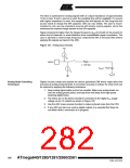
ADC Accuracy Definitions
An n-bit single-ended ADC converts a voltage linearly between GND and VREF in 2n
steps (LSBs). The lowest code is read as 0, and the highest code is read as 2n-1.
Several parameters describe the deviation from the ideal behavior:
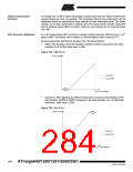
•
Offset: The deviation of the first transition (0x000 to 0x001) compared to the ideal
transition (at 0.5 LSB). Ideal value: 0 LSB.
Figure 124. Offset Error
Output Code
Ideal ADC
Actual ADC
Offset
Error
V
Input Voltage
REF
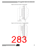
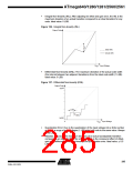
•
Gain Error: After adjusting for offset, the Gain Error is found as the deviation of the
last transition (0x3FE to 0x3FF) compared to the ideal transition (at 1.5 LSB below
maximum). Ideal value: 0 LSB
Figure 125. Gain Error
Gain
Error
Output Code
Ideal ADC
Actual ADC
VREF
Input Voltage
284
ATmega640/1280/1281/2560/2561
2549A–AVR–03/05

 ATMEL [ ATMEL ]