ATmega640/1280/1281/2560/2561
ADC Voltage Reference
The reference voltage for the ADC (VREF) indicates the conversion range for the ADC.
Single ended channels that exceed VREF will result in codes close to 0x3FF. VREF can be
selected as either AVCC, internal 1.1V reference, internal 2.56V reference or external
AREF pin.
AVCC is connected to the ADC through a passive switch. The internal 1.1V reference is
generated from the internal bandgap reference (VBG) through an internal amplifier. In
either case, the external AREF pin is directly connected to the ADC, and the reference
voltage can be made more immune to noise by connecting a capacitor between the
AREF pin and ground. VREF can also be measured at the AREF pin with a high impedant
voltmeter. Note that VREF is a high impedant source, and only a capacitive load should
be connected in a system. The Internal 2.56V reference is generated from the 1.1V
reference.
If the user has a fixed voltage source connected to the AREF pin, the user may not use
the other reference voltage options in the application, as they will be shorted to the
external voltage. If no external voltage is applied to the AREF pin, the user may switch
between AVCC, 1.1V and 2.56V as reference selection. The first ADC conversion result
after switching reference voltage source may be inaccurate, and the user is advised to
discard this result.
If differential channels are used, the selected reference should not be closer to AVCC
than indicated in “ADC Characteristics – Preliminary Data” on page 374.
ADC Noise Canceler
The ADC features a noise canceler that enables conversion during sleep mode to
reduce noise induced from the CPU core and other I/O peripherals. The noise canceler
can be used with ADC Noise Reduction and Idle mode. To make use of this feature, the
following procedure should be used:
1. Make sure that the ADC is enabled and is not busy converting. Single Con-
version mode must be selected and the ADC conversion complete interrupt
must be enabled.
2. Enter ADC Noise Reduction mode (or Idle mode). The ADC will start a con-
version once the CPU has been halted.
3. If no other interrupts occur before the ADC conversion completes, the ADC
interrupt will wake up the CPU and execute the ADC Conversion Complete
interrupt routine. If another interrupt wakes up the CPU before the ADC con-
version is complete, that interrupt will be executed, and an ADC Conversion
Complete interrupt request will be generated when the ADC conversion
completes. The CPU will remain in active mode until a new sleep command
is executed.
Note that the ADC will not be automatically turned off when entering other sleep modes
than Idle mode and ADC Noise Reduction mode. The user is advised to write zero to
ADEN before entering such sleep modes to avoid excessive power consumption.
If the ADC is enabled in such sleep modes and the user wants to perform differential
conversions, the user is advised to switch the ADC off and on after waking up from
sleep to prompt an extended conversion to get a valid result.
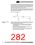
Analog Input Circuitry
The analog input circuitry for single ended channels is illustrated in Figure 121. An ana-
log source applied to ADCn is subjected to the pin capacitance and input leakage of that
pin, regardless of whether that channel is selected as input for the ADC. When the chan-
nel is selected, the source must drive the S/H capacitor through the series resistance
(combined resistance in the input path).
281
2549A–AVR–03/05

 ATMEL [ ATMEL ]