Changing Channel or
Reference Selection
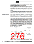
The MUXn and REFS1:0 bits in the ADMUX Register are single buffered through a tem-
porary register to which the CPU has random access. This ensures that the channels
and reference selection only takes place at a safe point during the conversion. The
channel and reference selection is continuously updated until a conversion is started.
Once the conversion starts, the channel and reference selection is locked to ensure a
sufficient sampling time for the ADC. Continuous updating resumes in the last ADC
clock cycle before the conversion completes (ADIF in ADCSRA is set). Note that the
conversion starts on the following rising ADC clock edge after ADSC is written. The user
is thus advised not to write new channel or reference selection values to ADMUX until
one ADC clock cycle after ADSC is written.
If Auto Triggering is used, the exact time of the triggering event can be indeterministic.
Special care must be taken when updating the ADMUX Register, in order to control
which conversion will be affected by the new settings.
If both ADATE and ADEN is written to one, an interrupt event can occur at any time. If
the ADMUX Register is changed in this period, the user cannot tell if the next conversion
is based on the old or the new settings. ADMUX can be safely updated in the following
ways:
1. When ADATE or ADEN is cleared.
2. During conversion, minimum one ADC clock cycle after the trigger event.
3. After a conversion, before the Interrupt Flag used as trigger source is
cleared.
When updating ADMUX in one of these conditions, the new settings will affect the next
ADC conversion.
Special care should be taken when changing differential channels. Once a differential
channel has been selected, the stage may take as much as TBD µs to stabilize to the
new value. Thus conversions should not be started within the first TBD µs after selecting
a new differential channel. Alternatively, conversion results obtained within this period
should be discarded.
The same settling time should be observed for the first differential conversion after
changing ADC reference (by changing the REFS1:0 bits in ADMUX).
ADC Input Channels
When changing channel selections, the user should observe the following guidelines to
ensure that the correct channel is selected:
In Single Conversion mode, always select the channel before starting the conversion.
The channel selection may be changed one ADC clock cycle after writing one to ADSC.
However, the simplest method is to wait for the conversion to complete before changing
the channel selection.
In Free Running mode, always select the channel before starting the first conversion.
The channel selection may be changed one ADC clock cycle after writing one to ADSC.
However, the simplest method is to wait for the first conversion to complete, and then
change the channel selection. Since the next conversion has already started automati-
cally, the next result will reflect the previous channel selection. Subsequent conversions
will reflect the new channel selection.
When switching to a differential gain channel, the first conversion result may have a
poor accuracy due to the required settling time for the automatic offset cancellation cir-
cuitry. The user should preferably disregard the first conversion result.
280
ATmega640/1280/1281/2560/2561
2549A–AVR–03/05

 ATMEL [ ATMEL ]