Receiver buffer FIFO will be flushed when the Receiver is disabled. Remaining data in
the buffer will be lost
Flushing the Receive Buffer
The receiver buffer FIFO will be flushed when the Receiver is disabled, i.e., the buffer
will be emptied of its contents. Unread data will be lost. If the buffer has to be flushed
during normal operation, due to for instance an error condition, read the UDRn I/O loca-
tion until the RXCn Flag is cleared. The following code example shows how to flush the
receive buffer.
Assembly Code Example(1)
USART_Flush:
sbis UCSRnA, RXCn
ret
in
r16, UDRn
rjmp USART_Flush
C Code Example(1)
void USART_Flush( void )
{
unsigned char dummy;
while ( UCSRnA & (1<<RXCn) ) dummy = UDRn;
}
Note:
1. See “About Code Examples” on page 8.
Asynchronous Data
Reception
The USART includes a clock recovery and a data recovery unit for handling asynchro-
nous data reception. The clock recovery logic is used for synchronizing the internally
generated baud rate clock to the incoming asynchronous serial frames at the RxDn pin.
The data recovery logic samples and low pass filters each incoming bit, thereby improv-
ing the noise immunity of the Receiver. The asynchronous reception operational range
depends on the accuracy of the internal baud rate clock, the rate of the incoming
frames, and the frame size in number of bits.
Asynchronous Clock
Recovery
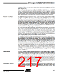
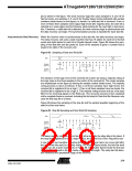
The clock recovery logic synchronizes internal clock to the incoming serial frames. Fig-
ure 87 illustrates the sampling process of the start bit of an incoming frame. The sample
rate is 16 times the baud rate for Normal mode, and eight times the baud rate for Double
Speed mode. The horizontal arrows illustrate the synchronization variation due to the
sampling process. Note the larger time variation when using the Double Speed mode
(U2Xn = 1) of operation. Samples denoted zero are samples done when the RxDn line
is idle (i.e., no communication activity).
Figure 87. Start Bit Sampling
RxD
IDLE
START
BIT 0
Sample
(U2X = 0)
0
0
1
1
2
3
2
4
5
3
6
7
4
8
9
5
10
11
6
12
13
7
14
15
8
16
1
1
2
3
Sample
(U2X = 1)
0
2
When the clock recovery logic detects a high (idle) to low (start) transition on the RxDn
line, the start bit detection sequence is initiated. Let sample 1 denote the first zero-sam-
218
ATmega640/1280/1281/2560/2561
2549A–AVR–03/05

 ATMEL [ ATMEL ]