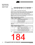
Table 92. Clock Select Bit Description
CS22
CS21
CS20
Description
0
0
0
0
1
1
1
1
0
0
1
1
0
0
1
1
0
1
0
1
0
1
0
1
No clock source (Timer/Counter stopped).
clkT2S/(No prescaling)
clkT2S/8 (From prescaler)
clkT2S/32 (From prescaler)
clkT2S/64 (From prescaler)
clkT2S/128 (From prescaler)
clkT S/256 (From prescaler)
2
clkT S/1024 (From prescaler)
2
If external pin modes are used for the Timer/Counter0, transitions on the T0 pin will
clock the counter even if the pin is configured as an output. This feature allows software
control of the counting.
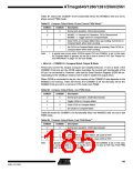
Timer/Counter Register –
TCNT2
Bit
7
6
5
4
3
2
1
0
TCNT2[7:0]
TCNT2
Read/Write
Initial Value
R/W
0
R/W
0
R/W
0
R/W
0
R/W
0
R/W
0
R/W
0
R/W
0
The Timer/Counter Register gives direct access, both for read and write operations, to
the Timer/Counter unit 8-bit counter. Writing to the TCNT2 Register blocks (removes)
the Compare Match on the following timer clock. Modifying the counter (TCNT2) while
the counter is running, introduces a risk of missing a Compare Match between TCNT2
and the OCR2x Registers.
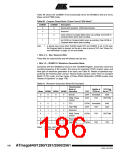
Output Compare Register A –
OCR2A
Bit
7
6
5
4
3
2
1
0
OCR2A[7:0]
R/W R/W
OCR2A
Read/Write
Initial Value
R/W
0
R/W
0
R/W
0
R/W
0
R/W
0
R/W
0
0
0
The Output Compare Register A contains an 8-bit value that is continuously compared
with the counter value (TCNT2). A match can be used to generate an Output Compare
interrupt, or to generate a waveform output on the OC2A pin.
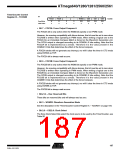
Output Compare Register B –
OCR2B
Bit
7
6
5
4
3
2
1
0
OCR2B[7:0]
R/W R/W
OCR2B
Read/Write
Initial Value
R/W
0
R/W
0
R/W
0
R/W
0
R/W
0
R/W
0
0
0
The Output Compare Register B contains an 8-bit value that is continuously compared
with the counter value (TCNT2). A match can be used to generate an Output Compare
interrupt, or to generate a waveform output on the OC2B pin.
188
ATmega640/1280/1281/2560/2561
2549A–AVR–03/05

 ATMEL [ ATMEL ]