ATmega8U2/16U2/32U2
the oscillator frequency. The oscillator can be calibrated to frequencies as specified in Table 26-
1 on page 266. Calibration outside that range is not guaranteed.
Note that this oscillator is used to time EEPROM and Flash write accesses, and these write
times will be affected accordingly. If the EEPROM or Flash are written, do not calibrate to more
than 8.8 MHz. Otherwise, the EEPROM or Flash write may fail.
The CAL7 bit determines the range of operation for the oscillator. Setting this bit to 0 gives the
lowest frequency range, setting this bit to 1 gives the highest frequency range. The two fre-
quency ranges are overlapping, in other words a setting of OSCCAL = 0x7F gives a higher
frequency than OSCCAL = 0x80.
The CAL[6:0] bits are used to tune the frequency within the selected range. A setting of 0x00
gives the lowest frequency in that range, and a setting of 0x7F gives the highest frequency in the
range.
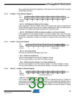
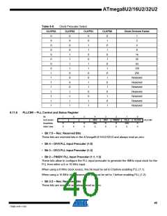
8.11.5
CLKPR – Clock Prescale Register
Bit
(0x61)
7
6
–
5
–
4
–
3
2
1
0
CLKPCE
CLKPS3
R/W
CLKPS2
R/W
CLKPS1
R/W
CLKPS0
R/W
CLKPR
Read/Write
Initial Value
R/W
0
R
0
R
0
R
0
See Bit Description
• Bit 7 – CLKPCE: Clock Prescaler Change Enable
The CLKPCE bit must be written to logic one to enable change of the CLKPS bits. The CLKPCE
bit is only updated when the other bits in CLKPR are simultaneously written to zero. CLKPCE is
cleared by hardware four cycles after it is written or when CLKPS bits are written. Rewriting the
CLKPCE bit within this time-out period does neither extend the time-out period, nor clear the
CLKPCE bit.
• Bit 6:4 - Reserved bits
These bits are reserved and will always read as zero.
• Bits 3:0 – CLKPS[3:0]: Clock Prescaler Select Bits 3 - 0
These bits define the division factor between the selected clock source and the internal system
clock. These bits can be written run-time to vary the clock frequency to suit the application
requirements. As the divider divides the master clock input to the MCU, the speed of all synchro-
nous peripherals is reduced when a division factor is used. The division factors are given in
Table 8-9.
The CKDIV8 Fuse determines the initial value of the CLKPS bits. If CKDIV8 is unprogrammed,
the CLKPS bits will be reset to “0000”. If CKDIV8 is programmed, CLKPS bits are reset to
“0011”, giving a division factor of 8 at start up. This feature should be used if the selected clock
source has a higher frequency than the maximum frequency of the device at the present operat-
ing conditions. Note that any value can be written to the CLKPS bits regardless of the CKDIV8
Fuse setting. The Application software must ensure that a sufficient division factor is chosen if
the selected clock source has a higher frequency than the maximum frequency of the device at
the present operating conditions. The device is shipped with the CKDIV8 Fuse programmed.
39
7799D–AVR–11/10

 ATMEL [ ATMEL ]