ATmega169P
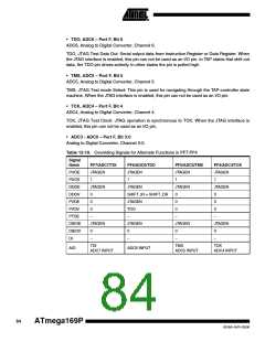
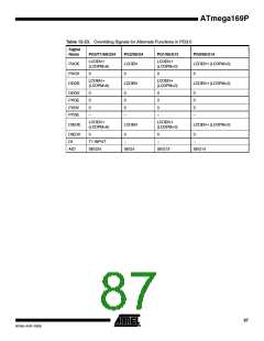
Table 12-20. Overriding Signals for Alternate Functions in PF3:PF0
Signal
Name
PUOE
PUOV
DDOE
DDOV
PVOE
PVOV
PTOE
DIEOE
DIEOV
DI
PF3/ADC3
PF2/ADC2
PF1/ADC1
PF0/ADC0
0
0
0
0
0
0
0
0
0
0
0
0
0
0
0
0
0
0
0
0
0
0
0
0
–
–
–
–
0
0
0
0
0
0
0
0
–
–
–
–
AIO
ADC3 INPUT
ADC2 INPUT
ADC1 INPUT
ADC0 INPUT
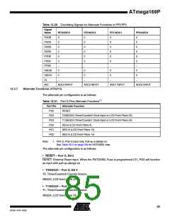
12.3.7
Alternate Functions of Port G
The alternate pin configuration is as follows:
Table 12-21. Port G Pins Alternate Functions(1)
Port Pin
PG5
Alternate Function
RESET
PG4
T0/SEG23 (Timer/Counter0 Clock Input or LCD Front Plane 23)
T1/SEG24 (Timer/Counter1 Clock Input or LCD Front Plane 24)
SEG4 (LCD Front Plane 4)
PG3
PG2
PG1
SEG13 (LCD Front Plane 13)
PG0
SEG14 (LCD Front Plane 14)
Note:
1. Port G, PG5 is input only. Pull-up is always on.
See Table 26-3 on page 296 for RSTDISBL fuse.
The alternate pin configuration is as follows:
• RESET – Port G, Bit 5
RESET: External Reset input. When the RSTDISBL Fuse is programmed (‘0’), PG5 will function
as input with pull-up always on.
• T0/SEG23 – Port G, Bit 4
T0, Timer/Counter0 Counter Source.
SEG23, LCD front plane 23
• T1/SEG24 – Port G, Bit 3
T1, Timer/Counter1 Counter Source.
SEG24, LCD front plane 24
85
8018A–AVR–03/06

 ATMEL [ ATMEL ]