ATmega169P
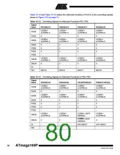
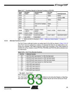
Table 12-17. Overriding Signals for Alternate Functions in PE3:PE0
Signal
Name
PE3/AIN1/
PCINT3
PE2/XCK/AIN0/
PCINT2
PE1/TXD/
PCINT1
PE0/RXD/PCINT0
PUOE
PUOV
DDOE
DDOV
PVOE
PVOV
PTOE
0
0
0
0
0
0
–
0
0
0
0
TXENn
RXENn
0
PORTE0 • PUD
TXENn
1
RXENn
0
0
0
–
XCK OUTPUT ENABLE TXENn
XCK
–
TXD
–
(PCINT3 • PCIE0)
+ AIN1D(1)
(PCINT2 • PCIE0) +
AIN0D(1)
DIEOE
PCINT1 • PCIE0
PCINT0 • PCIE0
DIEOV
DI
PCINT3 • PCIE0
PCINT3 INPUT
AIN1 INPUT
PCINT2 • PCIE0
XCK/PCINT2 INPUT
AIN0 INPUT
1
1
PCINT1 INPUT
–
RXD/PCINT0 INPUT
–
AIO
Note:
1. AIN0D and AIN1D is described in ”DIDR1 – Digital Input Disable Register 1” on page 214.
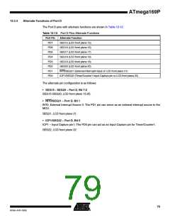
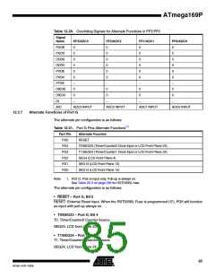
12.3.6
Alternate Functions of Port F
The Port F has an alternate function as analog input for the ADC as shown in Table 12-18. If
some Port F pins are configured as outputs, it is essential that these do not switch when a con-
version is in progress. This might corrupt the result of the conversion. If the JTAG interface is
enabled, the pull-up resistors on pins PF7(TDI), PF5(TMS) and PF4(TCK) will be activated even
if a reset occurs.
Table 12-18. Port F Pins Alternate Functions
Port Pin
PF7
Alternate Function
ADC7/TDI (ADC input channel 7 or JTAG Test Data Input)
ADC6/TDO (ADC input channel 6 or JTAG Test Data Output)
ADC5/TMS (ADC input channel 5 or JTAG Test mode Select)
ADC4/TCK (ADC input channel 4 or JTAG Test ClocK)
ADC3 (ADC input channel 3)
PF6
PF5
PF4
PF3
PF2
ADC2 (ADC input channel 2)
PF1
ADC1 (ADC input channel 1)
PF0
ADC0 (ADC input channel 0)
• TDI, ADC7 – Port F, Bit 7
ADC7, Analog to Digital Converter, Channel 7.
TDI, JTAG Test Data In: Serial input data to be shifted in to the Instruction Register or Data Reg-
ister (scan chains). When the JTAG interface is enabled, this pin can not be used as an I/O pin.
83
8018A–AVR–03/06

 ATMEL [ ATMEL ]