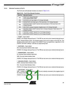
• XCK/AIN0/PCINT2 – Port E, Bit 2
XCK, USART External Clock. The Data Direction Register (DDE2) controls whether the clock is
output (DDE2 set) or input (DDE2 cleared). The XCK pin is active only when the USART oper-
ates in synchronous mode.
AIN0 – Analog Comparator Positive input. This pin is directly connected to the positive input of
the Analog Comparator.
PCINT2, Pin Change Interrupt Source 2: The PE2 pin can serve as an external interrupt source.
• TXD/PCINT1 – Port E, Bit 1
TXD0, UART0 Transmit pin.
PCINT1, Pin Change Interrupt Source 1: The PE1 pin can serve as an external interrupt source.
• RXD/PCINT0 – Port E, Bit 0
RXD, USART Receive pin. Receive Data (Data input pin for the USART). When the USART
Receiver is enabled this pin is configured as an input regardless of the value of DDE0. When the
USART forces this pin to be an input, a logical one in PORTE0 will turn on the internal pull-up.
PCINT0, Pin Change Interrupt Source 0: The PE0 pin can serve as an external interrupt source.
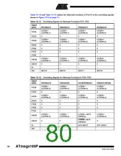
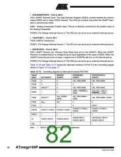
Table 12-16 and Table 12-17 relates the alternate functions of Port E to the overriding signals
shown in Figure 12-5 on page 71.
Table 12-16. Overriding Signals for Alternate Functions PE7:PE4
Signal
Name
PE6/DO/
PCINT6
PE5/DI/SDA/
PCINT5
PE4/USCK/SCL/
PCINT4
PE7/PCINT7
PUOE
PUOV
DDOE
0
0
0
0
USI_TWO-WIRE
0
USI_TWO-WIRE
0
0
CKOUT(1)
USI_TWO-WIRE
USI_TWO-WIRE
(SDA + PORTE5) •
DDE5
(USI_SCL_HOLD •
PORTE4) + DDE4
DDOV
PVOE
1
0
USI_THREE-
WIRE
USI_TWO-WIRE •
DDE5
CKOUT(1)
USI_TWO-WIRE • DDE4
PVOV
PTOE
clkI/O
–
DO
–
0
0
0
USITC
(PCINT5 • PCIE0) +
USISIE
(PCINT4 • PCIE0) +
USISIE
DIEOE
DIEOV
DI
PCINT7 • PCIE0 PCINT6 • PCIE0
1
1
1
1
DI/SDA INPUT
PCINT5 INPUT
USCKL/SCL INPUT
PCINT4 INPUT
PCINT7 INPUT
–
PCINT6 INPUT
–
AIO
–
–
Note:
1. CKOUT is one if the CKOUT Fuse is programmed
82
ATmega169P
8018A–AVR–03/06

 ATMEL [ ATMEL ]