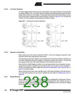
22.3.5
Low Power Waveform
To reduce toggle activity and hence power consumption a low power waveform can be selected
by writing LCDAB to one. Low power waveform requires two subsequent frames with the same
display data to obtain zero DC voltage. Consequently data latching and Interrupt Flag is only set
every second frame. Default and low power waveform is shown in Figure 22-7 for 1/3 duty and
1/3 bias. For other selections of duty and bias, the effect is similar.
Figure 22-7. Default and Low Power Waveform
VLCD
2/3VLCD
1/3VLCD
GND
VLCD
2/3VLCD
1/3VLCD
GND
SEG0
COM0
SEG0
COM0
VLCD
2/3VLCD
1/3VLCD
GND
VLCD
2/3VLCD
1/3VLCD
GND
VLCD
2/3VLCD
1/3VLCD
GND
-1/3VLCD
-2/3VLCD
-VLCD
VLCD
2/3VLCD
1/3VLCD
GND
-1/3VLCD
-2/3VLCD
-VLCD
SEG0 - COM0
SEG0 - COM0
Frame
Frame
Frame
Frame
22.3.6
Operation in Sleep Mode
When synchronous LCD clock is selected (LCDCS = 0) the LCD display will operate in Idle
mode and Power-save mode with any clock source.
An asynchronous clock from TOSC1 can be selected as LCD clock by writing the LCDCS bit to
one when Calibrated Internal RC Oscillator is selected as system clock source. The LCD will
then operate in Idle mode, ADC Noise Reduction mode and Power-save mode.
When EXCLK in ASSR Register is written to one, and asynchronous clock is selected, the exter-
nal clock input buffer is enabled and an external clock can be input on Timer Oscillator 1
(TOSC1) pin instead of a 32 kHz crystal. See ”Asynchronous operation of the Timer/Counter” on
page 150 for further details.
Before entering Power-down mode, Standby mode or ADC Noise Reduction mode with synchro-
nous LCD clock selected, the user have to disable the LCD. Refer to ”Disabling the LCD” on
page 242.
22.3.7
Display Blanking
When LCDBL is written to one, the LCD is blanked after completing the current frame. All seg-
ments and common pins are connected to GND, discharging the LCD. Display memory is
preserved. Display blanking should be used before disabling the LCD to avoid DC voltage
across segments, and a slowly fading image.
238
ATmega169P
8018A–AVR–03/06

 ATMEL [ ATMEL ]