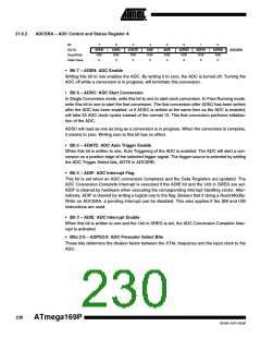
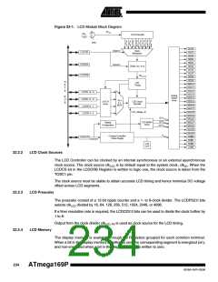
Figure 22-1. LCD Module Block Diagram
clkLCD
0
1
clki/o
12-bit Prescaler
TOSC
lcdcs
SEG0
SEG1
lcdps2:0
lcdcd2:0
Clock
Multiplexer
LCDFRR
SEG2
SEG3
SEG4
LCDCRA
LCDCRB
Divide by 1 to 8
SEG5
SEG6
SEG7
clkLCD_PS
SEG8
SEG9
D
A
T
A
LCD
Timing
SEG10
SEG11
SEG12
SEG13
SEG14
SEG15
SEG16
SEG17
SEG18
SEG19
SEG20
SEG21
SEG22
SEG23
SEG24
COM0
COM1
COM2
COM3
LCDDR 18 -15
LCDDR 13 -10
LCDDR 8 - 5
LCDDR 3 - 0
Analog
Switch
Array
B
U
S
25 x
4:1
MUX
LATCH
array
LCD Ouput
Decoder
LCD_voltage_ok
1/3 VLCD
1/2 VLCD
2/3 VLCD
LCD Buffer/
Driver
Display
Configuration
VLCD
Contrast Controller/
Power Supply
LCDCCR
lcdcc3:0
LCD
CAP
22.2.2
LCD Clock Sources
The LCD Controller can be clocked by an internal synchronous or an external asynchronous
clock source. The clock source clkLCD is by default equal to the system clock, clkI/O. When the
LCDCS bit in the LCDCRB Register is written to logic one, the clock source is taken from the
TOSC1 pin.
The clock source must be stable to obtain accurate LCD timing and hence minimize DC voltage
offset across LCD segments.
22.2.3
LCD Prescaler
The prescaler consist of a 12-bit ripple counter and a 1- to 8-clock divider. The LCDPS2:0 bits
selects clkLCD divided by 16, 64, 128, 256, 512, 1024, 2048, or 4096.
If a finer resolution rate is required, the LCDCD2:0 bits can be used to divide the clock further by
1 to 8.
Output from the clock divider clkLCD_PS is used as clock source for the LCD timing.
22.2.4
LCD Memory
The display memory is available through I/O Registers grouped for each common terminal.
When a bit in the display memory is written to one, the corresponding segment is energized (on),
and non-energized when a bit in the display memory is written to zero.
234
ATmega169P
8018A–AVR–03/06

 ATMEL [ ATMEL ]