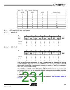
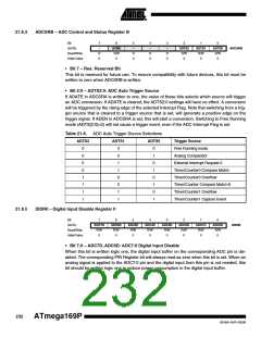
ATmega169P
To energize a segment, an absolute voltage above a certain threshold must be applied. This is
done by letting the output voltage on corresponding COM pin and SEG pin have opposite phase.
For display with more than one common, one (1/2 bias) or two (1/3 bias) additional voltage lev-
els must be applied. Otherwise, non-energized segments on COM0 would be energized for all
non-selected common.
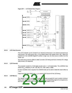
Addressing COM0 starts a frame by driving opposite phase with large amplitude out on COM0
compared to none addressed COM lines. Non-energized segments are in phase with the
addressed COM0, and energized segments have opposite phase and large amplitude. For
waveform figures refer to ”Mode of Operation” on page 236. Latched data from LCDDR4 -
LCDDR0 is multiplexed into the decoder. The decoder is controlled from the LCD timing and
sets up signals controlling the analog switches to produce an output waveform. Next, COM1 is
addressed, and latched data from LCDDR9 - LCDDR5 is input to decoder. Addressing continu-
ous until all COM lines are addressed according to number of common (duty). The display data
are latched before a new frame start.
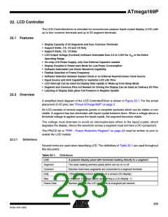
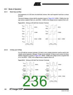
22.2.5
22.2.6
LCD Contrast Controller/Power Supply
The peak value (VLCD) on the output waveform determines the LCD Contrast. VLCD is controlled
by software from 2.6V to 3.35V independent of VCC. An internal signal inhibits output to the LCD
until VLCD has reached its target value.
LCDCAP
An external capacitor (typical > 470 nF) must be connected to the LCDCAP pin as shown in Fig-
ure 22-2. This capacitor acts as a reservoir for LCD power (VLCD). A large capacitance reduces
ripple on VLCD but increases the time until VLCD reaches its target value.
It is possible to use an external power supply. This power can be applied to LCDCAP before
V
CC. Externally applied VLCD can be both above and below VCC. Maximum VLCD is 5.5V
Figure 22-2. LCDCAP Connection
62
63
64
1
2
3
LCDCAP
VLCD
(Optional)
22.2.7
LCD Buffer Driver
Intermediate voltage levels are generated from buffers/drivers. The buffers are active the
amount of time specified by LCDDC[2:0] in ”LCDCCR – LCD Contrast Control Register” on page
248. Then LCD output pins are tri-stated and buffers are switched off. Shortening the drive time
will reduce power consumption, but displays with high internal resistance or capacitance may
need longer drive time to achieve sufficient contrast.
235
8018A–AVR–03/06

 ATMEL [ ATMEL ]