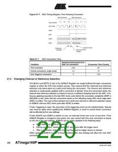
21.6.3
ADC Accuracy Definitions
An n-bit single-ended ADC converts a voltage linearly between GND and VREF in 2n steps
(LSBs). The lowest code is read as 0, and the highest code is read as 2n-1.
Several parameters describe the deviation from the ideal behavior:
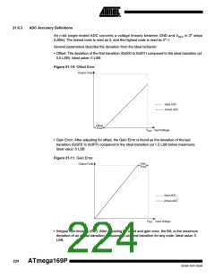
• Offset: The deviation of the first transition (0x000 to 0x001) compared to the ideal transition (at
0.5 LSB). Ideal value: 0 LSB.
Figure 21-10. Offset Error
Output Code
Ideal ADC
Actual ADC
Offset
Error
VREF
Input Voltage
• Gain Error: After adjusting for offset, the Gain Error is found as the deviation of the last
transition (0x3FE to 0x3FF) compared to the ideal transition (at 1.5 LSB below maximum).
Ideal value: 0 LSB
Figure 21-11. Gain Error
Gain
Error
Output Code
Ideal ADC
Actual ADC
VREF
Input Voltage
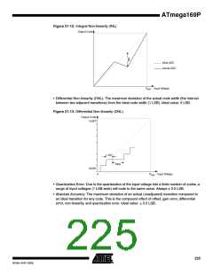
• Integral Non-linearity (INL): After adjusting for offset and gain error, the INL is the maximum
deviation of an actual transition compared to an ideal transition for any code. Ideal value: 0
LSB.
224
ATmega169P
8018A–AVR–03/06

 ATMEL [ ATMEL ]