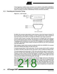
21.6.1
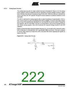
Analog Input Circuitry
The analog input circuitry for single ended channels is illustrated in Figure 21-8. An analog
source applied to ADCn is subjected to the pin capacitance and input leakage of that pin, regard-
less of whether that channel is selected as input for the ADC. When the channel is selected, the
source must drive the S/H capacitor through the series resistance (combined resistance in the
input path).
The ADC is optimized for analog signals with an output impedance of approximately 10 kΩ or
less. If such a source is used, the sampling time will be negligible. If a source with higher imped-
ance is used, the sampling time will depend on how long time the source needs to charge the
S/H capacitor, with can vary widely. The user is recommended to only use low impedant sources
with slowly varying signals, since this minimizes the required charge transfer to the S/H
capacitor.
Signal components higher than the Nyquist frequency (fADC/2) should not be present for either
kind of channels, to avoid distortion from unpredictable signal convolution. The user is advised
to remove high frequency components with a low-pass filter before applying the signals as
inputs to the ADC.
Figure 21-8. Analog Input Circuitry
IIH
ADCn
1..100 kW
CS/H= 14 pF
IIL
VCC/2
222
ATmega169P
8018A–AVR–03/06

 ATMEL [ ATMEL ]