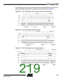
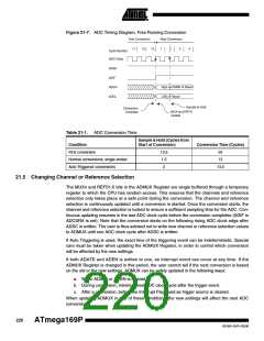
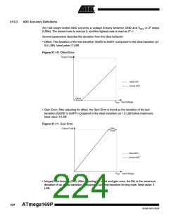
Figure 21-7. ADC Timing Diagram, Free Running Conversion
One Conversion
Next Conversion
11
12
13
1
2
3
4
Cycle Number
ADC Clock
ADSC
ADIF
ADCH
ADCL
Sign and MSB of Result
LSB of Result
Sample & Hold
Conversion
Complete
MUX and REFS
Update
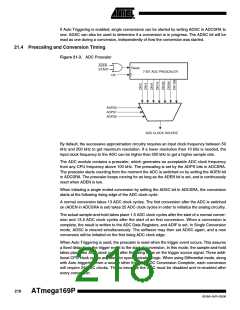
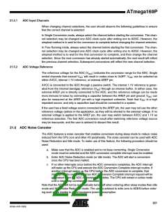
Table 21-1. ADC Conversion Time
Sample & Hold (Cycles from
Start of Conversion)
Condition
Conversion Time (Cycles)
First conversion
13.5
1.5
2
25
13
Normal conversions, single ended
Auto Triggered conversions
13.5
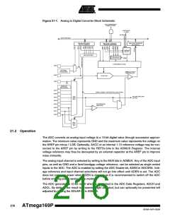
21.5 Changing Channel or Reference Selection
The MUXn and REFS1:0 bits in the ADMUX Register are single buffered through a temporary
register to which the CPU has random access. This ensures that the channels and reference
selection only takes place at a safe point during the conversion. The channel and reference
selection is continuously updated until a conversion is started. Once the conversion starts, the
channel and reference selection is locked to ensure a sufficient sampling time for the ADC. Con-
tinuous updating resumes in the last ADC clock cycle before the conversion completes (ADIF in
ADCSRA is set). Note that the conversion starts on the following rising ADC clock edge after
ADSC is written. The user is thus advised not to write new channel or reference selection values
to ADMUX until one ADC clock cycle after ADSC is written.
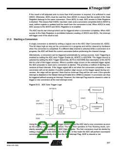
If Auto Triggering is used, the exact time of the triggering event can be indeterministic. Special
care must be taken when updating the ADMUX Register, in order to control which conversion
will be affected by the new settings.
If both ADATE and ADEN is written to one, an interrupt event can occur at any time. If the
ADMUX Register is changed in this period, the user cannot tell if the next conversion is based
on the old or the new settings. ADMUX can be safely updated in the following ways:
a. When ADATE or ADEN is cleared.
b. During conversion, minimum one ADC clock cycle after the trigger event.
c. After a conversion, before the Interrupt Flag used as trigger source is cleared.
When updating ADMUX in one of these conditions, the new settings will affect the next ADC
conversion.
220
ATmega169P
8018A–AVR–03/06

 ATMEL [ ATMEL ]