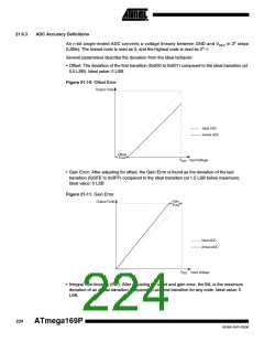
21.8 ADC Register Description
21.8.1
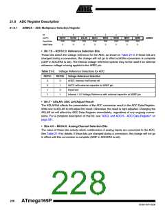
ADMUX – ADC Multiplexer Selection Register
Bit
7
REFS1
R/W
0
6
REFS0
R/W
0
5
ADLAR
R/W
0
4
MUX4
R/W
0
3
MUX3
R/W
0
2
MUX2
R/W
0
1
MUX1
R/W
0
0
MUX0
R/W
0
(0x7C)
ADMUX
Read/Write
Initial Value
• Bit 7:6 – REFS1:0: Reference Selection Bits
These bits select the voltage reference for the ADC, as shown in Table 21-3. If these bits are
changed during a conversion, the change will not go in effect until this conversion is complete
(ADIF in ADCSRA is set). The internal voltage reference options may not be used if an external
reference voltage is being applied to the AREF pin.
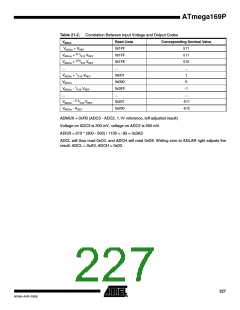
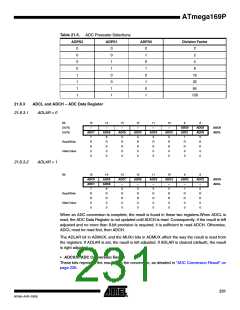
Table 21-3. Voltage Reference Selections for ADC
REFS1
REFS0
Voltage Reference Selection
0
0
1
1
0
1
0
1
AREF, Internal Vref turned off
AVCC with external capacitor at AREF pin
Reserved
Internal 1.1V Voltage Reference with external capacitor at AREF pin
• Bit 5 – ADLAR: ADC Left Adjust Result
The ADLAR bit affects the presentation of the ADC conversion result in the ADC Data Register.
Write one to ADLAR to left adjust the result. Otherwise, the result is right adjusted. Changing the
ADLAR bit will affect the ADC Data Register immediately, regardless of any ongoing conver-
sions. For a complete description of this bit, see ”ADCL and ADCH – ADC Data Register” on
page 231.
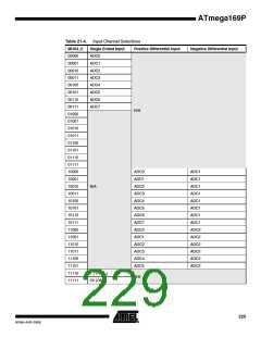
• Bits 4:0 – MUX4:0: Analog Channel Selection Bits
The value of these bits selects which combination of analog inputs are connected to the ADC.
See Table 21-4 for details. If these bits are changed during a conversion, the change will not go
in effect until this conversion is complete (ADIF in ADCSRA is set).
228
ATmega169P
8018A–AVR–03/06

 ATMEL [ ATMEL ]