ATmega169P
21.6.2
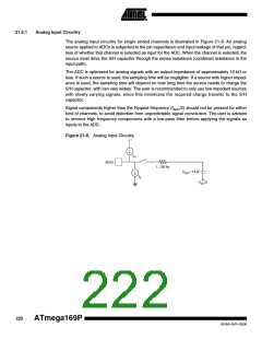
Analog Noise Canceling Techniques
Digital circuitry inside and outside the device generates EMI which might affect the accuracy of
analog measurements. If conversion accuracy is critical, the noise level can be reduced by
applying the following techniques:
a. Keep analog signal paths as short as possible. Make sure analog tracks run over the
analog ground plane, and keep them well away from high-speed switching digital
tracks.
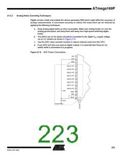
b. The AVCC pin on the device should be connected to the digital VCC supply voltage
via an LC network as shown in Figure 21-9.
c. Use the ADC noise canceler function to reduce induced noise from the CPU.
d. If any ADC port pins are used as digital outputs, it is essential that these do not
switch while a conversion is in progress.
Figure 21-9. ADC Power Connections
PA0 51
VCC
52
GND
53
(ADC7) PF7 54
(ADC6) PF6 55
(ADC5) PF5 56
(ADC4) PF4 57
(ADC3) PF3 58
(ADC2) PF2 59
(ADC1) PF1
(ADC0) PF0
60
61
10µΗ
62
63
64
AREF
GND
AVCC
100nF
1
Ground Plane
223
8018A–AVR–03/06

 ATMEL [ ATMEL ]