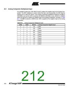
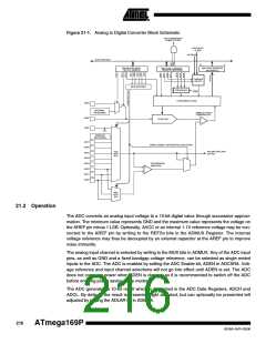
Figure 21-1. Analog to Digital Converter Block Schematic
ADC CONVERSION
COMPLETE IRQ
INTERRUPT
FLAGS
ADTS[2:0]
8-BIT DATA BUS
15
0
ADC MULTIPLEXER
SELECT (ADMUX)
ADC CTRL. & STATUS
REGISTER (ADCSRA)
ADC DATA REGISTER
(ADCH/ADCL)
TRIGGER
SELECT
MUX DECODER
PRESCALER
START
CONVERSION LOGIC
AVCC
INTERNAL
REFERENCE
SAMPLE & HOLD
COMPARATOR
AREF
GND
10-BIT DAC
-
+
BANDGAP
REFERENCE
ADC7
ADC6
ADC5
ADC4
ADC3
ADC2
ADC1
ADC0
SINGLE ENDED / DIFFERENTIAL SELECTION
POS.
INPUT
MUX
ADC MULTIPLEXER
OUTPUT
DIFFERENTIAL
AMPLIFIER
+
-
NEG.
INPUT
MUX
21.2 Operation
The ADC converts an analog input voltage to a 10-bit digital value through successive approxi-
mation. The minimum value represents GND and the maximum value represents the voltage on
the AREF pin minus 1 LSB. Optionally, AVCC or an internal 1.1V reference voltage may be con-
nected to the AREF pin by writing to the REFSn bits in the ADMUX Register. The internal
voltage reference may thus be decoupled by an external capacitor at the AREF pin to improve
noise immunity.
The analog input channel is selected by writing to the MUX bits in ADMUX. Any of the ADC input
pins, as well as GND and a fixed bandgap voltage reference, can be selected as single ended
inputs to the ADC. The ADC is enabled by setting the ADC Enable bit, ADEN in ADCSRA. Volt-
age reference and input channel selections will not go into effect until ADEN is set. The ADC
does not consume power when ADEN is cleared, so it is recommended to switch off the ADC
before entering power saving sleep modes.
The ADC generates a 10-bit result which is presented in the ADC Data Registers, ADCH and
ADCL. By default, the result is presented right adjusted, but can optionally be presented left
adjusted by setting the ADLAR bit in ADMUX.
216
ATmega169P
8018A–AVR–03/06

 ATMEL [ ATMEL ]