ATmega169P
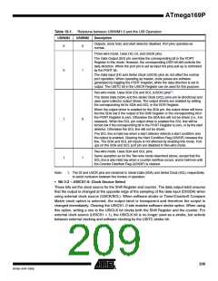
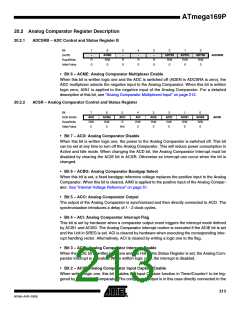
Table 19-1. Relations between USIWM1:0 and the USI Operation
USIWM1
USIWM0
Description
Outputs, clock hold, and start detector disabled. Port pins operates as
normal.
0
0
Three-wire mode. Uses DO, DI, and USCK pins.
The Data Output (DO) pin overrides the corresponding bit in the PORT
Register in this mode. However, the corresponding DDR bit still controls the
data direction. When the port pin is set as input the pins pull-up is controlled
by the PORT bit.
0
1
The Data Input (DI) and Serial Clock (USCK) pins do not affect the normal
port operation. When operating as master, clock pulses are software
generated by toggling the PORT Register, while the data direction is set to
output. The USITC bit in the USICR Register can be used for this purpose.
Two-wire mode. Uses SDA (DI) and SCL (USCK) pins(1)
.
The Serial Data (SDA) and the Serial Clock (SCL) pins are bi-directional and
uses open-collector output drives. The output drivers are enabled by setting
the corresponding bit for SDA and SCL in the DDR Register.
When the output driver is enabled for the SDA pin, the output driver will force
the line SDA low if the output of the Shift Register or the corresponding bit in
the PORT Register is zero. Otherwise the SDA line will not be driven (i.e., it is
released). When the SCL pin output driver is enabled the SCL line will be
forced low if the corresponding bit in the PORT Register is zero, or by the start
detector. Otherwise the SCL line will not be driven.
1
0
The SCL line is held low when a start detector detects a start condition and
the output is enabled. Clearing the Start Condition Flag (USISIF) releases the
line. The SDA and SCL pin inputs is not affected by enabling this mode. Pull-
ups on the SDA and SCL port pin are disabled in Two-wire mode.
Two-wire mode. Uses SDA and SCL pins.
Same operation as for the Two-wire mode described above, except that the
SCL line is also held low when a counter overflow occurs, and is held low until
the Counter Overflow Flag (USIOIF) is cleared.
1
1
Note:
1. The DI and USCK pins are renamed to Serial Data (SDA) and Serial Clock (SCL) respectively
to avoid confusion between the modes of operation.
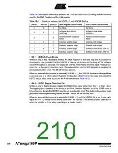
• Bit 3:2 – USICS1:0: Clock Source Select
These bits set the clock source for the Shift Register and counter. The data output latch ensures
that the output is changed at the opposite edge of the sampling of the data input (DI/SDA) when
using external clock source (USCK/SCL). When software strobe or Timer/Counter0 Compare
Match clock option is selected, the output latch is transparent and therefore the output is
changed immediately. Clearing the USICS1..0 bits enables software strobe option. When using
this option, writing a one to the USICLK bit clocks both the Shift Register and the counter. For
external clock source (USICS1 = 1), the USICLK bit is no longer used as a strobe, but selects
between external clocking and software clocking by the USITC strobe bit.
209
8018A–AVR–03/06

 ATMEL [ ATMEL ]