ATmega169P
19.4 USI Register Descriptions
19.4.1
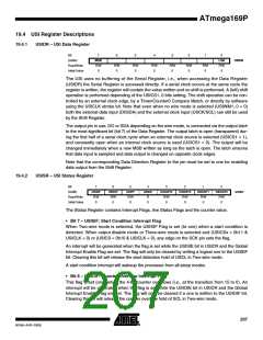
USIDR – USI Data Register
Bit
7
6
5
4
3
2
1
0
(0xBA)
MSB
R/W
0
LSB
R/W
0
USIDR
Read/Write
Initial Value
R/W
0
R/W
0
R/W
0
R/W
0
R/W
0
R/W
0
The USI uses no buffering of the Serial Register, i.e., when accessing the Data Register
(USIDR) the Serial Register is accessed directly. If a serial clock occurs at the same cycle the
register is written, the register will contain the value written and no shift is performed. A (left) shift
operation is performed depending of the USICS1..0 bits setting. The shift operation can be con-
trolled by an external clock edge, by a Timer/Counter0 Compare Match, or directly by software
using the USICLK strobe bit. Note that even when no wire mode is selected (USIWM1..0 = 0)
both the external data input (DI/SDA) and the external clock input (USCK/SCL) can still be used
by the Shift Register.
The output pin in use, DO or SDA depending on the wire mode, is connected via the output latch
to the most significant bit (bit 7) of the Data Register. The output latch is open (transparent) dur-
ing the first half of a serial clock cycle when an external clock source is selected (USICS1 = 1),
and constantly open when an internal clock source is used (USICS1 = 0). The output will be
changed immediately when a new MSB written as long as the latch is open. The latch ensures
that data input is sampled and data output is changed on opposite clock edges.
Note that the corresponding Data Direction Register to the pin must be set to one for enabling
data output from the Shift Register.
19.4.2
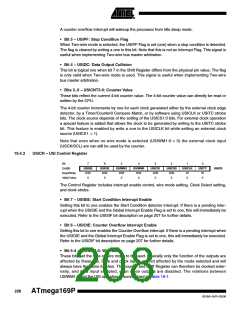
USISR – USI Status Register
Bit
7
6
USIOIF
R/W
0
5
USIPF
R/W
0
4
USIDC
R
3
USICNT3
R/W
2
USICNT2
R/W
1
USICNT1
R/W
0
USICNT0
R/W
USISIF
R/W
0
USISR
(0xB9)
Read/Write
Initial Value
0
0
0
0
0
The Status Register contains Interrupt Flags, line Status Flags and the counter value.
• Bit 7 – USISIF: Start Condition Interrupt Flag
When Two-wire mode is selected, the USISIF Flag is set (to one) when a start condition is
detected. When output disable mode or Three-wire mode is selected and (USICSx = 0b11 &
USICLK = 0) or (USICS = 0b10 & USICLK = 0), any edge on the SCK pin sets the flag.
An interrupt will be generated when the flag is set while the USISIE bit in USICR and the Global
Interrupt Enable Flag are set. The flag will only be cleared by writing a logical one to the USISIF
bit. Clearing this bit will release the start detection hold of USCL in Two-wire mode.
A start condition interrupt will wakeup the processor from all sleep modes.
• Bit 6 – USIOIF: Counter Overflow Interrupt Flag
This flag is set (one) when the 4-bit counter overflows (i.e., at the transition from 15 to 0). An
interrupt will be generated when the flag is set while the USIOIE bit in USICR and the Global
Interrupt Enable Flag are set. The flag will only be cleared if a one is written to the USIOIF bit.
Clearing this bit will release the counter overflow hold of SCL in Two-wire mode.
207
8018A–AVR–03/06

 ATMEL [ ATMEL ]