ATmega169P
20.2 Analog Comparator Register Description
20.2.1
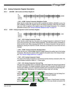
ADCSRB – ADC Control and Status Register B
Bit
7
–
6
ACME
R/W
0
5
–
4
–
3
–
2
ADTS2
R/W
0
1
ADTS1
R/W
0
0
ADTS0
R/W
0
(0x7B)
ADCSRB
Read/Write
Initial Value
R
0
R
0
R
0
R
0
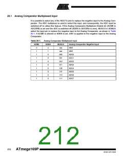
• Bit 6 – ACME: Analog Comparator Multiplexer Enable
When this bit is written logic one and the ADC is switched off (ADEN in ADCSRA is zero), the
ADC multiplexer selects the negative input to the Analog Comparator. When this bit is written
logic zero, AIN1 is applied to the negative input of the Analog Comparator. For a detailed
description of this bit, see ”Analog Comparator Multiplexed Input” on page 212.
20.2.2
ACSR – Analog Comparator Control and Status Register
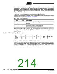
Bit
0x30 (0x50)
7
6
5
4
3
ACIE
R/W
0
2
ACIC
R/W
0
1
ACIS1
R/W
0
0
ACIS0
R/W
0
ACD
ACBG
ACO
ACI
R/W
0
ACSR
Read/Write
Initial Value
R/W
0
R/W
0
R
N/A
• Bit 7 – ACD: Analog Comparator Disable
When this bit is written logic one, the power to the Analog Comparator is switched off. This bit
can be set at any time to turn off the Analog Comparator. This will reduce power consumption in
Active and Idle mode. When changing the ACD bit, the Analog Comparator Interrupt must be
disabled by clearing the ACIE bit in ACSR. Otherwise an interrupt can occur when the bit is
changed.
• Bit 6 – ACBG: Analog Comparator Bandgap Select
When this bit is set, a fixed bandgap reference voltage replaces the positive input to the Analog
Comparator. When this bit is cleared, AIN0 is applied to the positive input of the Analog Compar-
ator. See ”Internal Voltage Reference” on page 51.
• Bit 5 – ACO: Analog Comparator Output
The output of the Analog Comparator is synchronized and then directly connected to ACO. The
synchronization introduces a delay of 1 - 2 clock cycles.
• Bit 4 – ACI: Analog Comparator Interrupt Flag
This bit is set by hardware when a comparator output event triggers the interrupt mode defined
by ACIS1 and ACIS0. The Analog Comparator interrupt routine is executed if the ACIE bit is set
and the I-bit in SREG is set. ACI is cleared by hardware when executing the corresponding inter-
rupt handling vector. Alternatively, ACI is cleared by writing a logic one to the flag.
• Bit 3 – ACIE: Analog Comparator Interrupt Enable
When the ACIE bit is written logic one and the I-bit in the Status Register is set, the Analog Com-
parator interrupt is activated. When written logic zero, the interrupt is disabled.
• Bit 2 – ACIC: Analog Comparator Input Capture Enable
When written logic one, this bit enables the Input Capture function in Timer/Counter1 to be trig-
gered by the Analog Comparator. The comparator output is in this case directly connected to the
213
8018A–AVR–03/06

 ATMEL [ ATMEL ]