ATmega169P
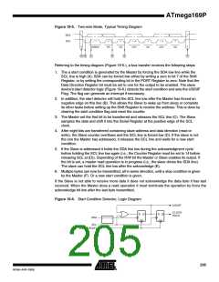
Figure 19-5. Two-wire Mode, Typical Timing Diagram
SDA
1 - 7
8
9
1 - 8
9
1 - 8
9
SCL
S
P
ADDRESS
R/W
ACK
DATA
ACK
DATA
ACK
A
B
C
D
E
F
Referring to the timing diagram (Figure 19-5.), a bus transfer involves the following steps:
1. The a start condition is generated by the Master by forcing the SDA low line while the
SCL line is high (A). SDA can be forced low either by writing a zero to bit 7 of the Shift
Register, or by setting the corresponding bit in the PORT Register to zero. Note that the
Data Direction Register bit must be set to one for the output to be enabled. The slave
device’s start detector logic (Figure 19-6.) detects the start condition and sets the USISIF
Flag. The flag can generate an interrupt if necessary.
2. In addition, the start detector will hold the SCL line low after the Master has forced an
negative edge on this line (B). This allows the Slave to wake up from sleep or complete
its other tasks before setting up the Shift Register to receive the address. This is done by
clearing the start condition flag and reset the counter.
3. The Master set the first bit to be transferred and releases the SCL line (C). The Slave
samples the data and shift it into the Serial Register at the positive edge of the SCL
clock.
4. After eight bits are transferred containing slave address and data direction (read or
write), the Slave counter overflows and the SCL line is forced low (D). If the slave is not
the one the Master has addressed, it releases the SCL line and waits for a new start
condition.
5. If the Slave is addressed it holds the SDA line low during the acknowledgment cycle
before holding the SCL line low again (i.e., the Counter Register must be set to 14 before
releasing SCL at (D)). Depending of the R/W bit the Master or Slave enables its output. If
the bit is set, a master read operation is in progress (i.e., the slave drives the SDA line)
The slave can hold the SCL line low after the acknowledge (E).
6. Multiple bytes can now be transmitted, all in same direction, until a stop condition is given
by the Master (F). Or a new start condition is given.
If the Slave is not able to receive more data it does not acknowledge the data byte it has last
received. When the Master does a read operation it must terminate the operation by force the
acknowledge bit low after the last byte transmitted.
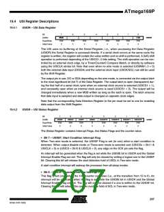
Figure 19-6. Start Condition Detector, Logic Diagram
USISIF
CLOCK
HOLD
D Q
D Q
SDA
CLR
CLR
SCL
Write( USISIF)
205
8018A–AVR–03/06

 ATMEL [ ATMEL ]