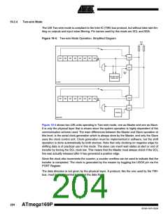
A counter overflow interrupt will wakeup the processor from Idle sleep mode.
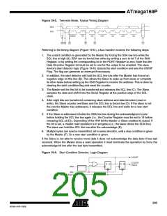
• Bit 5 – USIPF: Stop Condition Flag
When Two-wire mode is selected, the USIPF Flag is set (one) when a stop condition is detected.
The flag is cleared by writing a one to this bit. Note that this is not an Interrupt Flag. This signal is
useful when implementing Two-wire bus master arbitration.
• Bit 4 – USIDC: Data Output Collision
This bit is logical one when bit 7 in the Shift Register differs from the physical pin value. The flag
is only valid when Two-wire mode is used. This signal is useful when implementing Two-wire
bus master arbitration.
• Bits 3..0 – USICNT3:0: Counter Value
These bits reflect the current 4-bit counter value. The 4-bit counter value can directly be read or
written by the CPU.
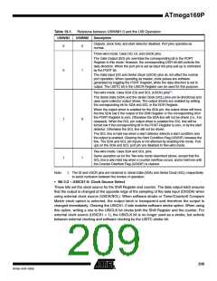
The 4-bit counter increments by one for each clock generated either by the external clock edge
detector, by a Timer/Counter0 Compare Match, or by software using USICLK or USITC strobe
bits. The clock source depends of the setting of the USICS1:0 bits. For external clock operation
a special feature is added that allows the clock to be generated by writing to the USITC strobe
bit. This feature is enabled by write a one to the USICLK bit while setting an external clock
source (USICS1 = 1).
Note that even when no wire mode is selected (USIWM1:0 = 0) the external clock input
(USCK/SCL) are can still be used by the counter.
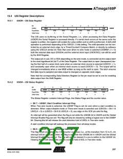
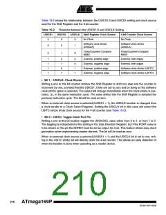
19.4.3
USICR – USI Control Register
Bit
7
USISIE
R/W
0
6
USIOIE
R/W
0
5
USIWM1
R/W
4
USIWM0
R/W
3
USICS1
R/W
0
2
USICS0
R/W
0
1
0
USITC
W
(0xB8)
USICLK
USICR
Read/Write
Initial Value
W
0
0
0
0
The Control Register includes interrupt enable control, wire mode setting, Clock Select setting,
and clock strobe.
• Bit 7 – USISIE: Start Condition Interrupt Enable
Setting this bit to one enables the Start Condition detector interrupt. If there is a pending inter-
rupt when the USISIE and the Global Interrupt Enable Flag is set to one, this will immediately be
executed. Refer to the USISIF bit description on page 207 for further details.
• Bit 6 – USIOIE: Counter Overflow Interrupt Enable
Setting this bit to one enables the Counter Overflow interrupt. If there is a pending interrupt when
the USIOIE and the Global Interrupt Enable Flag is set to one, this will immediately be executed.
Refer to the USIOIF bit description on page 207 for further details.
• Bit 5:4 – USIWM1:0: Wire Mode
These bits set the type of wire mode to be used. Basically only the function of the outputs are
affected by these bits. Data and clock inputs are not affected by the mode selected and will
always have the same function. The counter and Shift Register can therefore be clocked exter-
nally, and data input sampled, even when outputs are disabled. The relations between
USIWM1:0 and the USI operation is summarized in Table 19-1.
208
ATmega169P
8018A–AVR–03/06

 ATMEL [ ATMEL ]