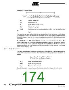
18.1.1
AVR USART vs. AVR UART – Compatibility
The USART is fully compatible with the AVR UART regarding:
• Bit locations inside all USART Registers.
• Baud Rate Generation.
• Transmitter Operation.
• Transmit Buffer Functionality.
• Receiver Operation.
However, the receive buffering has two improvements that will affect the compatibility in some
special cases:
• A second Buffer Register has been added. The two Buffer Registers operate as a circular FIFO
buffer. Therefore the UDRn must only be read once for each incoming data! More important is
the fact that the Error Flags (FEn and DORn) and the ninth data bit (RXB8n) are buffered with
the data in the receive buffer. Therefore the status bits must always be read before the UDRn
Register is read. Otherwise the error status will be lost since the buffer state is lost.
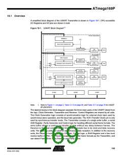
• The Receiver Shift Register can now act as a third buffer level. This is done by allowing the
received data to remain in the serial Shift Register (see Figure 18-1) if the Buffer Registers are
full, until a new start bit is detected. The USART is therefore more resistant to Data OverRun
(DORn) error conditions.
The following control bits have changed name, but have same functionality and register location:
• CHR9 is changed to UCSZn2.
• OR is changed to DORn.
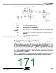
18.2 Clock Generation
The Clock Generation logic generates the base clock for the Transmitter and Receiver. The
USART supports four modes of clock operation: Normal asynchronous, Double Speed asyn-
chronous, Master synchronous and Slave synchronous mode. The UMSELn bit in USART
Control and Status Register C (UCSRnC) selects between asynchronous and synchronous
operation. Double Speed (asynchronous mode only) is controlled by the U2Xn found in the
UCSRnA Register. When using synchronous mode (UMSELn = 1), the Data Direction Register
for the XCK pin (DDR_XCK) controls whether the clock source is internal (Master mode) or
external (Slave mode). The XCK pin is only active when using synchronous mode.
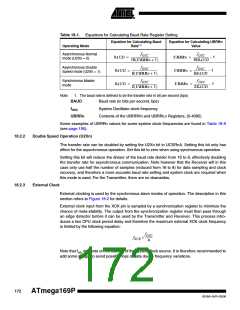
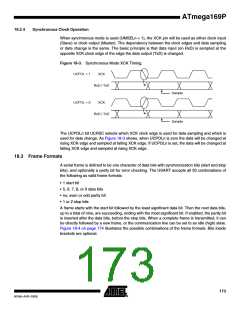
Figure 18-2 shows a block diagram of the clock generation logic.
170
ATmega169P
8018A–AVR–03/06

 ATMEL [ ATMEL ]