17. SPI – Serial Peripheral Interface
The Serial Peripheral Interface (SPI) allows high-speed synchronous data transfer between the
ATmega169P and peripheral devices or between several AVR devices. The ATmega169P SPI
includes the following features:
• Full-duplex, Three-wire Synchronous Data Transfer
• Master or Slave Operation
• LSB First or MSB First Data Transfer
• Seven Programmable Bit Rates
• End of Transmission Interrupt Flag
• Write Collision Flag Protection
• Wake-up from Idle Mode
• Double Speed (CK/2) Master SPI Mode
The PRSPI bit in ”PRR – Power Reduction Register” on page 44 must be written to zero to
enable SPI module.
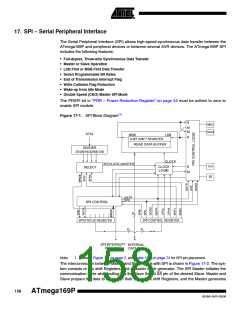
Figure 17-1. SPI Block Diagram(1)
DIVIDER
/2/4/8/16/32/64/128
Note:
1. Refer to Figure 1-1 on page 2, and Table 12-6 on page 74 for SPI pin placement.
The interconnection between Master and Slave CPUs with SPI is shown in Figure 17-2. The sys-
tem consists of two shift Registers, and a Master clock generator. The SPI Master initiates the
communication cycle when pulling low the Slave Select SS pin of the desired Slave. Master and
Slave prepare the data to be sent in their respective shift Registers, and the Master generates
158
ATmega169P
8018A–AVR–03/06

 ATMEL [ ATMEL ]