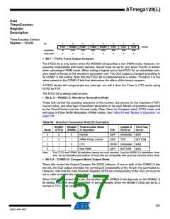
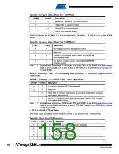
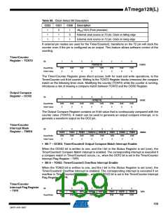
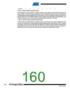
ATmega128(L)
Output
Compare
Modulator
(OCM1C2)
Overview
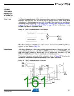
The Output Compare Modulator (OCM) allows generation of waveforms modulated with a carrier
frequency. The modulator uses the outputs from the Output Compare Unit C of the 16-bit
Timer/Counter1 and the Output Compare Unit of the 8-bit Timer/Counter2. For more details
about these Timer/Counters see “16-bit Timer/Counter (Timer/Counter1 and Timer/Counter3)”
on page 112 and “8-bit Timer/Counter2 with PWM” on page 145. Note that this feature is not
available in ATmega103 compatibility mode.
Figure 72. Output Compare Modulator, Block Diagram
OC1C
OC2
Timer/Counter 1
Timer/Counter 2
Pin
OC1C /
OC2 / PB7
When the modulator is enabled, the two output compare channels are modulated together as
shown in the block diagram (Figure 72).
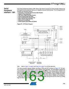
Description
The Output Compare unit 1C and Output Compare unit 2 shares the PB7 port pin for output. The
outputs of the Output Compare units (OC1C and OC2) overrides the normal PORTB7 Register
when one of them is enabled (i.e., when COMnx1:0 is not equal to zero). When both OC1C and
OC2 are enabled at the same time, the modulator is automatically enabled.
The functional equivalent schematic of the modulator is shown on Figure 73. The schematic
includes part of the Timer/Counter units and the port B pin 7 output driver circuit.
Figure 73. Output Compare Modulator, Schematic
COM21
COM20
Vcc
COM1C1
COM1C0
Modulator
0
1
( From Waveform Generator )
D
Q
1
0
OC1C
Pin
OC1C /
OC2 / PB7
( From Waveform Generator )
D
Q
Q
OC2
D
D
Q
PORTB7
DDRB7
DATABUS
161
2467P–AVR–08/07

 ATMEL [ ATMEL ]