ATmega128(L)
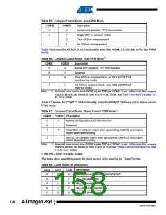
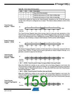
Table 68. Clock Select Bit Description
CS22
CS21
CS20
Description
1
1
1
0
1
1
1
0
1
clkI/O/1024 (From prescaler)
External clock source on T2 pin. Clock on falling edge
External clock source on T2 pin. Clock on rising edge
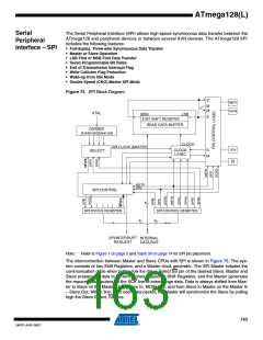
If external pin modes are used for the Timer/Counter2, transitions on the T2 pin will clock the
counter even if the pin is configured as an output. This feature allows software control of the
counting.
Timer/Counter
Register – TCNT2
Bit
7
6
5
4
3
2
1
0
TCNT2[7:0]
TCNT2
Read/Write
Initial Value
R/W
0
R/W
0
R/W
0
R/W
0
R/W
0
R/W
0
R/W
0
R/W
0
The Timer/Counter Register gives direct access, both for read and write operations, to the
Timer/Counter unit 8-bit counter. Writing to the TCNT2 Register blocks (removes) the compare
match on the following timer clock. Modifying the counter (TCNT2) while the counter is running,
introduces a risk of missing a compare match between TCNT2 and the OCR2 Register.
Output Compare
Register – OCR2
Bit
7
6
5
4
3
2
1
0
OCR2[7:0]
OCR2
Read/Write
Initial Value
R/W
0
R/W
0
R/W
0
R/W
0
R/W
0
R/W
0
R/W
0
R/W
0
The Output Compare Register contains an 8-bit value that is continuously compared with the
counter value (TCNT2). A match can be used to generate an output compare interrupt, or to
generate a waveform output on the OC2 pin.
Timer/Counter
Interrupt Mask
Register – TIMSK
Bit
7
OCIE2
R/W
0
6
TOIE2
R/W
0
5
TICIE1
R/W
0
4
OCIE1A
R/W
0
3
OCIE1B
R/W
0
2
TOIE1
R/W
0
1
OCIE0
R/W
0
0
TOIE0
R/W
0
TIMSK
Read/Write
Initial Value
• Bit 7 – OCIE2: Timer/Counter2 Output Compare Match Interrupt Enable
When the OCIE2 bit is written to one, and the I-bit in the Status Register is set (one), the
Timer/Counter2 Compare Match interrupt is enabled. The corresponding interrupt is executed if
a compare match in Timer/Counter2 occurs, i.e., when the OCF2 bit is set in the Timer/Counter
Interrupt Flag Register – TIFR.
• Bit 6 – TOIE2: Timer/Counter2 Overflow Interrupt Enable
When the TOIE2 bit is written to one, and the I-bit in the Status Register is set (one), the
Timer/Counter2 Overflow interrupt is enabled. The corresponding interrupt is executed if an
overflow in Timer/Counter2 occurs, i.e., when the TOV2 bit is set in the Timer/Counter Interrupt
Flag Register – TIFR.
Timer/Counter
Interrupt Flag Register
– TIFR
Bit
7
6
5
4
3
2
1
0
OCF2
R/W
TOV2
R/W
ICF1
R/W
OCF1A
R/W
OCF1B
R/W
TOV1
R/W
OCF0
R/W
TOV0
R/W
TIFR
Read/Write
159
2467P–AVR–08/07

 ATMEL [ ATMEL ]