ATmega128(L)
Timer/Counter
Timing Diagrams
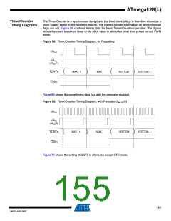
The Timer/Counter is a synchronous design and the timer clock (clkT2) is therefore shown as a
clock enable signal in the following figures. The figures include information on when interrupt
flags are set. Figure 68 contains timing data for basic Timer/Counter operation. The figure
shows the count sequence close to the MAX value in all modes other than phase correct PWM
mode.
Figure 68. Timer/Counter Timing Diagram, no Prescaling
clkI/O
clkTn
(clkI/O/1)
TCNTn
TOVn
MAX - 1
MAX
BOTTOM
BOTTOM + 1
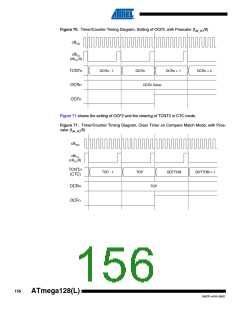
Figure 69 shows the same timing data, but with the prescaler enabled.
Figure 69. Timer/Counter Timing Diagram, with Prescaler (fclk_I/O/8)
clkI/O
clkTn
(clkI/O/8)
TCNTn
TOVn
MAX - 1
MAX
BOTTOM
BOTTOM + 1
Figure 70 shows the setting of OCF2 in all modes except CTC mode.
155
2467P–AVR–08/07

 ATMEL [ ATMEL ]