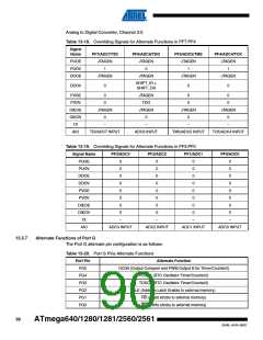
ATmega640/1280/1281/2560/2561
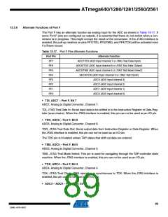
13.3.6
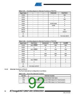
Alternate Functions of Port F
The Port F has an alternate function as analog input for the ADC as shown in Table 13-17. If
some Port F pins are configured as outputs, it is essential that these do not switch when a con-
version is in progress. This might corrupt the result of the conversion. If the JTAG interface is
enabled, the pull-up resistors on pins PF7(TDI), PF5(TMS), and PF4(TCK) will be activated even
if a Reset occurs.
Table 13-17. Port F Pins Alternate Functions
Port Pin
PF7
Alternate Function
ADC7/TDI (ADC input channel 7 or JTAG Test Data Input)
ADC6/TDO (ADC input channel 6 or JTAG Test Data Output)
ADC5/TMS (ADC input channel 5 or JTAG Test Mode Select)
ADC4/TCK (ADC input channel 4 or JTAG Test ClocK)
ADC3 (ADC input channel 3)
PF6
PF5
PF4
PF3
PF2
ADC2 (ADC input channel 2)
PF1
ADC1 (ADC input channel 1)
PF0
ADC0 (ADC input channel 0)
• TDI, ADC7 – Port F, Bit 7
ADC7, Analog to Digital Converter, Channel 7.
TDI, JTAG Test Data In: Serial input data to be shifted in to the Instruction Register or Data Reg-
ister (scan chains). When the JTAG interface is enabled, this pin can not be used as an I/O pin.
• TDO, ADC6 – Port F, Bit 6
ADC6, Analog to Digital Converter, Channel 6.
TDO, JTAG Test Data Out: Serial output data from Instruction Register or Data Register. When
the JTAG interface is enabled, this pin can not be used as an I/O pin.
The TDO pin is tri-stated unless TAP states that shift out data are entered.
• TMS, ADC5 – Port F, Bit 5
ADC5, Analog to Digital Converter, Channel 5.
TMS, JTAG Test Mode Select: This pin is used for navigating through the TAP-controller state
machine. When the JTAG interface is enabled, this pin can not be used as an I/O pin.
• TCK, ADC4 – Port F, Bit 4
ADC4, Analog to Digital Converter, Channel 4.
TCK, JTAG Test Clock: JTAG operation is synchronous to TCK. When the JTAG interface is
enabled, this pin can not be used as an I/O pin.
• ADC3 – ADC0 – Port F, Bit 3:0
89
2549L–AVR–08/07

 ATMEL [ ATMEL ]