ATmega640/1280/1281/2560/2561
• AIN1/OC3A – Port E, Bit 3
AIN1 – Analog Comparator Negative input. This pin is directly connected to the negative input of
the Analog Comparator.
OC3A, Output Compare Match A output: The PE3 pin can serve as an External output for the
Timer/Counter3 Output Compare A. The pin has to be configured as an output (DDE3 set “one”)
to serve this function. The OC3A pin is also the output pin for the PWM mode timer function.
• AIN0/XCK0 – Port E, Bit 2
AIN0 – Analog Comparator Positive input. This pin is directly connected to the positive input of
the Analog Comparator.
XCK0, USART0 External clock. The Data Direction Register (DDE2) controls whether the clock
is output (DDE2 set) or input (DDE2 cleared). The XCK0 pin is active only when the USART0
operates in Synchronous mode.
• PDO/TXD0 – Port E, Bit 1
PDO, SPI Serial Programming Data Output. During Serial Program Downloading, this pin is
used as data output line for the ATmega1281/2561. For ATmega640/1280/2560 this function is
placed on MISO.
TXD0, USART0 Transmit pin.
• PDI/RXD0/PCINT8 – Port E, Bit 0
PDI, SPI Serial Programming Data Input. During Serial Program Downloading, this pin is used
as data input line for the ATmega1281/2561. For ATmega640/1280/2560 this function is placed
on MOSI.
RXD0, USART0 Receive Pin. Receive Data (Data input pin for the USART0). When the
USART0 receiver is enabled this pin is configured as an input regardless of the value of DDRE0.
When the USART0 forces this pin to be an input, a logical one in PORTE0 will turn on the inter-
nal pull-up.
PCINT8, Pin Change Interrupt source 8: The PE0 pin can serve as an external interrupt source.
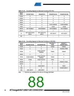
Table 13-15 and Table 13-16 relates the alternate functions of Port E to the overriding signals
shown in Figure 13-5 on page 76.
87
2549L–AVR–08/07

 ATMEL [ ATMEL ]