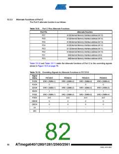
13.3.5
Alternate Functions of Port E
The Port E pins with alternate functions are shown in Table 13-14.
Table 13-14. Port E Pins Alternate Functions
Port Pin
Alternate Function
INT7/ICP3/CLK0 (External Interrupt 7 Input, Timer/Counter3 Input Capture Trigger or
PE7
Divided System Clock)
PE6
INT6/ T3 (External Interrupt 6 Input or Timer/Counter3 Clock Input)
INT5/OC3C (External Interrupt 5 Input or Output Compare and PWM Output C for
PE5
Timer/Counter3)
INT4/OC3B (External Interrupt4 Input or Output Compare and PWM Output B for
PE4
PE3
Timer/Counter3)
AIN1/OC3A (Analog Comparator Negative Input or Output Compare and PWM Output A for
Timer/Counter3)
PE2
PE1
AIN0/XCK0 (Analog Comparator Positive Input or USART0 external clock input/output)
PDO(1)/TXD0 (Programming Data Output or USART0 Transmit Pin)
PDI(1)/RXD0/PCINT8 (Programming Data Input, USART0 Receive Pin or Pin Change
PE0
Interrupt 8)
Note:
1. Only for ATmega1281/2561. For ATmega640/1280/2560 these functions are placed on
MISO/MOSI pins.
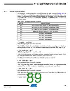
• INT7/ICP3/CLKO – Port E, Bit 7
INT7, External Interrupt source 7: The PE7 pin can serve as an external interrupt source.
ICP3, Input Capture Pin 3: The PE7 pin can act as an input capture pin for Timer/Counter3.
CLKO - Divided System Clock: The divided system clock can be output on the PE7 pin. The
divided system clock will be output if the CKOUT Fuse is programmed, regardless of the
PORTE7 and DDE7 settings. It will also be output during reset.
• INT6/T3 – Port E, Bit 6
INT6, External Interrupt source 6: The PE6 pin can serve as an external interrupt source.
T3, Timer/Counter3 counter source.
• INT5/OC3C – Port E, Bit 5
INT5, External Interrupt source 5: The PE5 pin can serve as an External Interrupt source.
OC3C, Output Compare Match C output: The PE5 pin can serve as an External output for the
Timer/Counter3 Output Compare C. The pin has to be configured as an output (DDE5 set “one”)
to serve this function. The OC3C pin is also the output pin for the PWM mode timer function.
• INT4/OC3B – Port E, Bit 4
INT4, External Interrupt source 4: The PE4 pin can serve as an External Interrupt source.
OC3B, Output Compare Match B output: The PE4 pin can serve as an External output for the
Timer/Counter3 Output Compare B. The pin has to be configured as an output (DDE4 set (one))
to serve this function. The OC3B pin is also the output pin for the PWM mode timer function.
86
ATmega640/1280/1281/2560/2561
2549L–AVR–08/07

 ATMEL [ ATMEL ]