ger source that is cleared to a trigger source that is set, will generate a positive edge on the
trigger signal. If ADEN in ADCSRA is set, this will start a conversion. Switching to Free Running
mode (ADTS[2:0]=0) will not cause a trigger event, even if the ADC Interrupt Flag is set.
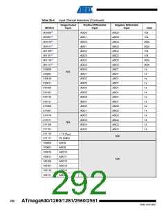
Table 26-6. ADC Auto Trigger Source Selections
ADTS2
ADTS1
ADTS0
Trigger Source
0
0
0
0
1
1
1
1
0
0
1
1
0
0
1
1
0
1
0
1
0
1
0
1
Free Running mode
Analog Comparator
External Interrupt Request 0
Timer/Counter0 Compare Match A
Timer/Counter0 Overflow
Timer/Counter1 Compare Match B
Timer/Counter1 Overflow
Timer/Counter1 Capture Event
Note:
Free running mode cannot be used for differential channels. (See chapter “Differential Channels”
on page 28126.4.1)
26.8.6
DIDR0 – Digital Input Disable Register 0
Bit
7
ADC7D
R/W
0
6
ADC6D
R/W
0
5
ADC5D
R/W
0
4
ADC4D
R/W
0
3
ADC3D
R/W
0
2
ADC2D
R/W
0
1
ADC1D
R/W
0
0
ADC0D
R/W
0
(0x7E)
DIDR0
Read/Write
Initial Value
• Bit 7:0 – ADC7D:ADC0D: ADC7:0 Digital Input Disable
When this bit is written logic one, the digital input buffer on the corresponding ADC pin is dis-
abled. The corresponding PIN Register bit will always read as zero when this bit is set. When an
analog signal is applied to the ADC7:0 pin and the digital input from this pin is not needed, this
bit should be written logic one to reduce power consumption in the digital input buffer.
26.8.7
DIDR2 – Digital Input Disable Register 2
Bit
(0x7D)
7
6
5
ADC13D
R/W
4
ADC12D
R/W
3
ADC11D
R/W
2
ADC10D
R/W
1
ADC9D
R/W
0
0
ADC8D
R/W
0
ADC15D
ADC14D
DIDR2
Read/Write
R/W
R/W
Initial Value
0
0
0
0
0
0
• Bit 7:0 – ADC15D:ADC8D: ADC15:8 Digital Input Disable
When this bit is written logic one, the digital input buffer on the corresponding ADC pin is dis-
abled. The corresponding PIN Register bit will always read as zero when this bit is set. When an
analog signal is applied to the ADC15:8 pin and the digital input from this pin is not needed, this
bit should be written logic one to reduce power consumption in the digital input buffer.
296
ATmega640/1280/1281/2560/2561
2549L–AVR–08/07

 ATMEL [ ATMEL ]