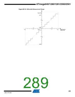
ATmega640/1280/1281/2560/2561
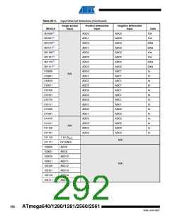
Table 26-4. Input Channel Selections (Continued)
Single Ended
Input
Positive Differential
Input
Negative Differential
Input
MUX5:0
101000(1)
101001(1)
101010(1)
101011(1)
101100(1)
101101(1)
101110(1)
101111(1)
110000
110001
110010
110011
110100
110101
110110
110111
111000
111001
111010
111011
111100
111101
111110
111111
Gain
10x
ADC8
ADC8
ADC9
ADC8
ADC8
ADC8
ADC10
ADC10
ADC10
ADC10
ADC9
ADC9
ADC9
ADC9
ADC9
ADC9
ADC9
ADC9
ADC10
ADC10
ADC10
ADC10
ADC10
ADC10
N/A
10x
200x
200x
10x
10x
200x
200x
1x
ADC8
ADC9
ADC10
ADC11
ADC10
ADC11
ADC8
ADC9
1x
N/A
ADC10
ADC11
ADC12
ADC13
ADC14
ADC15
ADC8
1x
1x
1x
1x
1x
1x
1x
ADC9
1x
ADC10
ADC11
ADC12
ADC13
1x
1x
1x
N/A
Reserved
Reserved
1x
N/A
Note:
1. To reach the given accuracy, 10x or 200x Gain should not be used for operating voltage below
2.7V
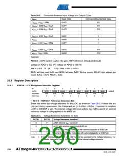
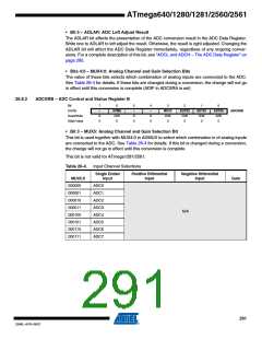
26.8.3
ADCSRA – ADC Control and Status Register A
Bit
7
ADEN
R/W
0
6
ADSC
R/W
0
5
ADATE
R/W
0
4
ADIF
R/W
0
3
ADIE
R/W
0
2
ADPS2
R/W
0
1
ADPS1
R/W
0
0
ADPS0
R/W
0
(0x7A)
ADCSRA
Read/Write
Initial Value
• Bit 7 – ADEN: ADC Enable
Writing this bit to one enables the ADC. By writing it to zero, the ADC is turned off. Turning the
ADC off while a conversion is in progress, will terminate this conversion.
293
2549L–AVR–08/07

 ATMEL [ ATMEL ]