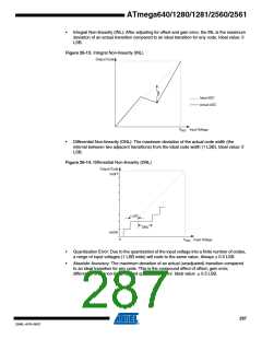
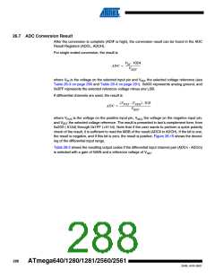
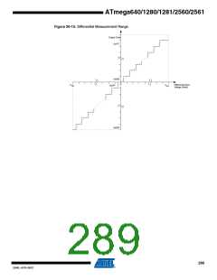
ATmega640/1280/1281/2560/2561
• Bit 5 – ADLAR: ADC Left Adjust Result
The ADLAR bit affects the presentation of the ADC conversion result in the ADC Data Register.
Write one to ADLAR to left adjust the result. Otherwise, the result is right adjusted. Changing the
ADLAR bit will affect the ADC Data Register immediately, regardless of any ongoing conver-
sions. For a complete description of this bit, see “ADCL and ADCH – The ADC Data Register” on
page 295.
• Bits 4:0 – MUX4:0: Analog Channel and Gain Selection Bits
The value of these bits selects which combination of analog inputs are connected to the ADC.
See Table 26-4 for details. If these bits are changed during a conversion, the change will not go
in effect until this conversion is complete (ADIF in ADCSRA is set)
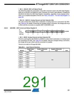
26.8.2
ADCSRB – ADC Control and Status Register B
Bit
(0x7B)
7
6
5
–
4
–
3
MUX5
R/W
0
2
ADTS2
R/W
0
1
ADTS1
R/W
0
0
ADTS0
R/W
0
–
ACME
ADCSRB
Read/Write
R
0
R/W
R
0
R
0
Initial Value
0
• Bit 3 – MUX5: Analog Channel and Gain Selection Bit
This bit is used together with MUX4:0 in ADMUX to select which combination in of analog inputs
are connected to the ADC. See Table 26-4 for details. If this bit is changed during a conversion,
the change will not go in effect until this conversion is complete.
This bit is not valid for ATmega1281/2561.
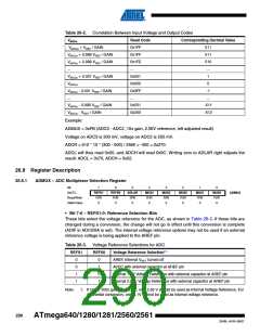
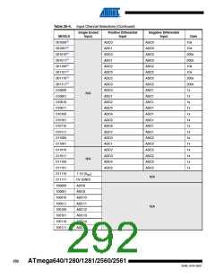
Table 26-4. Input Channel Selections
Single Ended
Input
Positive Differential
Input
Negative Differential
Input
MUX5:0
000000
000001
000010
000011
000100
000101
000110
000111
Gain
ADC0
ADC1
ADC2
ADC3
ADC4
ADC5
ADC6
ADC7
N/A
291
2549L–AVR–08/07

 ATMEL [ ATMEL ]