ATmega640/1280/1281/2560/2561
8.3.1
EEPROM Read/Write Access
The EEPROM Access Registers are accessible in the I/O space, see “Register Description” on
page 34.
The write access time for the EEPROM is given in Table 8-4 on page 23. A self-timing function,
however, lets the user software detect when the next byte can be written. If the user code con-
tains instructions that write the EEPROM, some precautions must be taken. In heavily filtered
power supplies, VCC is likely to rise or fall slowly on power-up/down. This causes the device for
some period of time to run at a voltage lower than specified as minimum for the clock frequency
used. See “Preventing EEPROM Corruption” on page 25. for details on how to avoid problems in
these situations.
In order to prevent unintentional EEPROM writes, a specific write procedure must be followed.
See the description of the EEPROM Control Register for details on this, “Register Description”
on page 34.
When the EEPROM is read, the CPU is halted for four clock cycles before the next instruction is
executed. When the EEPROM is written, the CPU is halted for two clock cycles before the next
instruction is executed.
The calibrated Oscillator is used to time the EEPROM accesses. Table 8-4 lists the typical pro-
gramming time for EEPROM access from the CPU.
Figure 8-4. EEPROM Programming Time
Symbol
Number of Calibrated RC Oscillator Cycles
Typ Programming Time
EEPROM write
(from CPU)
26,368
3.3 ms
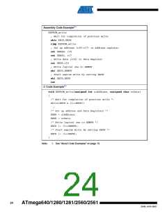
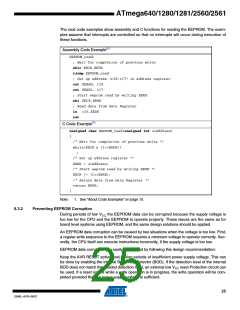
The following code examples show one assembly and one C function for writing to the
EEPROM. The examples assume that interrupts are controlled (e.g. by disabling interrupts glo-
bally) so that no interrupts will occur during execution of these functions. The examples also
assume that no Flash Boot Loader is present in the software. If such code is present, the
EEPROM write function must also wait for any ongoing SPM command to finish.
23
2549L–AVR–08/07

 ATMEL [ ATMEL ]