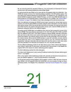
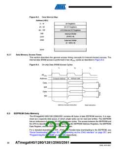
Figure 8-2. Data Memory Map
Address (HEX)
0 - 1F
32 Registers
64 I/O Registers
20 - 5F
60 - 1FF
200
416 External I/O Registers
Internal SRAM
(8192 x 8)
21FF
2200
External SRAM
(0 - 64K x 8)
FFFF
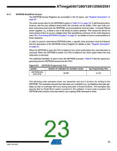
8.2.1
Data Memory Access Times
This section describes the general access timing concepts for internal memory access. The
internal data SRAM access is performed in two clkCPU cycles as described in Figure 8-3.
Figure 8-3. On-chip Data SRAM Access Cycles
T1
T2
T3
clkCPU
Address valid
Compute Address
Address
Data
WR
Data
RD
Memory Access Instruction
Next Instruction
8.3
EEPROM Data Memory
The ATmega640/1280/1281/2560/2561 contains 4K bytes of data EEPROM memory. It is orga-
nized as a separate data space, in which single bytes can be read and written. The EEPROM
has an endurance of at least 100,000 write/erase cycles. The access between the EEPROM and
the CPU is described in the following, specifying the EEPROM Address Registers, the EEPROM
Data Register, and the EEPROM Control Register.
For a detailed description of SPI, JTAG and Parallel data downloading to the EEPROM, see
“Serial Downloading” on page 351, “Programming via the JTAG Interface” on page 357, and
“Programming the EEPROM” on page 345 respectively.
22
ATmega640/1280/1281/2560/2561
2549L–AVR–08/07

 ATMEL [ ATMEL ]