8. AVR Memories
This section describes the different memories in the ATmega640/1280/1281/2560/2561. The
AVR architecture has two main memory spaces, the Data Memory and the Program Memory
space. In addition, the ATmega640/1280/1281/2560/2561 features an EEPROM Memory for
data storage. All three memory spaces are linear and regular.
8.1
In-System Reprogrammable Flash Program Memory
The ATmega640/1280/1281/2560/2561 contains 64K/128K/256K bytes On-chip In-System
Reprogrammable Flash memory for program storage, see Table 8-1 on page 20. Since all AVR
instructions are 16 or 32 bits wide, the Flash is organized as 32K/64K/128K x 16. For software
security, the Flash Program memory space is divided into two sections, Boot Program section
and Application Program section.
The Flash memory has an endurance of at least 10,000 write/erase cycles. The
ATmega640/1280/1281/2560/2561 Program Counter (PC) is 15/16/17 bits wide, thus addressing
the 32K/64K/128K program memory locations. The operation of Boot Program section and asso-
ciated Boot Lock bits for software protection are described in detail in “Boot Loader Support –
Read-While-Write Self-Programming” on page 318. “Memory Programming” on page 337 con-
tains a detailed description on Flash data serial downloading using the SPI pins or the JTAG
interface.
Constant tables can be allocated within the entire program memory address space (see the LPM
– Load Program Memory instruction description and ELPM - Extended Load Program Memory
instruction description).
Timing diagrams for instruction fetch and execution are presented in “Instruction Execution Tim-
ing” on page 16.
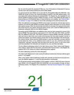
Figure 8-1. Program Flash Memory Map
Address (HEX)
0
Application Flash Section
Boot Flash Section
0x7FFF/0xFFFF/0x1FFFF
8.2
SRAM Data Memory
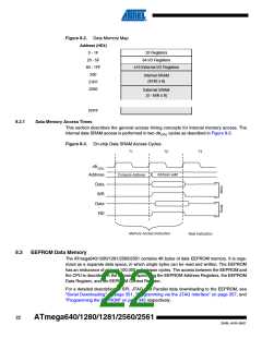
Table 8-2 on page 22 shows how the ATmega640/1280/1281/2560/2561 SRAM Memory is
organized.
The ATmega640/1280/1281/2560/2561 is a complex microcontroller with more peripheral units
than can be supported within the 64 location reserved in the Opcode for the IN and OUT instruc-
tions. For the Extended I/O space from $060 - $1FF in SRAM, only the ST/STS/STD and
LD/LDS/LDD instructions can be used.
The first 4,608/8,704 Data Memory locations address both the Register File, the I/O Memory,
Extended I/O Memory, and the internal data SRAM. The first 32 locations address the Register
20
ATmega640/1280/1281/2560/2561
2549L–AVR–08/07

 ATMEL [ ATMEL ]