ATmega640/1280/1281/2560/2561
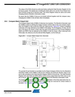
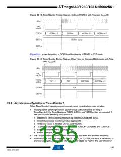
Figure 20-10. Timer/Counter Timing Diagram, Setting of OCF2A, with Prescaler (fclk_I/O/8)
clkI/O
clkTn
(clkI/O/8)
TCNTn
OCRnx
OCFnx
OCRnx - 1
OCRnx
OCRnx + 1
OCRnx + 2
OCRnx Value
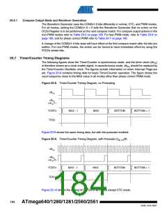
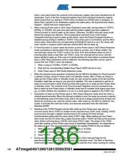
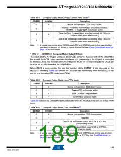
Figure 20-11 shows the setting of OCF2A and the clearing of TCNT2 in CTC mode.
Figure 20-11. Timer/Counter Timing Diagram, Clear Timer on Compare Match mode, with Pres-
caler (fclk_I/O/8)
clkI/O
clkTn
(clkI/O/8)
TCNTn
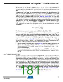
(CTC)
TOP - 1
TOP
BOTTOM
BOTTOM + 1
OCRnx
TOP
OCFnx
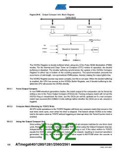
20.8 Asynchronous Operation of Timer/Counter2
When Timer/Counter2 operates asynchronously, some considerations must be taken.
•
Warning: When switching between asynchronous and synchronous clocking of
Timer/Counter2, the Timer Registers TCNT2, OCR2x, and TCCR2x might be corrupted. A
safe procedure for switching clock source is:
1. Disable the Timer/Counter2 interrupts by clearing OCIE2x and TOIE2.
2. Select clock source by setting AS2 as appropriate.
3. Write new values to TCNT2, OCR2x, and TCCR2x.
4. To switch to asynchronous operation: Wait for TCN2UB, OCR2xUB, and TCR2xUB.
5. Clear the Timer/Counter2 Interrupt Flags.
6. Enable interrupts, if needed.
•
•
The CPU main clock frequency must be more than four times the Oscillator frequency.
When writing to one of the registers TCNT2, OCR2x, or TCCR2x, the value is transferred to
a temporary register, and latched after two positive edges on TOSC1. The user should not
185
2549L–AVR–08/07

 ATMEL [ ATMEL ]